Industry Directory | Manufacturer
We are a manufacturer of Reed Switches, SMD Reed Sensors and other customized Magnetic sensing solutions, incorporated in 1971.
New Equipment | Education/Training
This specification covers qualification and performance of rigid PCBs including with or without plated-through holes, single-sided, double-sided, multilayer with or without blind/buried vias and metal core boards. It addresses final finish and surfac
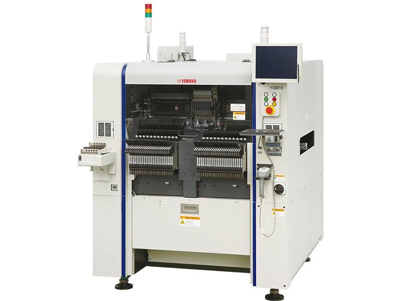
Yamaha YSM10 Pick and Place High-Speed Modular SMT Placement Yamaha fastest SMT placement machines , Yamaha SMT Pick and Place Machine, Yamaha Chip mounter, for SMT assembly system. Applicable PCB L 510 x W 460mm - L 50 x W
Industry News | 2003-03-11 08:45:00.0
CAMtastic DXP is the latest version of Altium's complete CAM verification and editing system that bridges the gap between PCB design and manufacturing and facilitates communication between board designers, fabrication engineers, and their clients.
Industry News | 2023-10-23 09:44:34.0
Changes address advances in rigid printed board fabrication processes
Technical Library | 2019-07-17 17:56:34.0
The increased demand for electronic devices in recent years has led to an extensive research in the field to meet the requirements of the industry. Electrolytic copper has been an important technology in the fabrication of PCBs and semiconductors. Aqueous sulfuric acid baths are explored for filling or building up with copper structures like blind micro vias (BMV), trenches, through holes (TH), and pillar bumps. As circuit miniaturization continues, developing a process that simultaneously fills vias and plates TH with various sizes and aspect ratios, while minimizing the surface copper thickness is critical. Filling BMV and plating TH at the same time, presents great difficulties for the PCB manufactures. The conventional copper plating processes that provide good via fill and leveling of the deposit tend to worsen the throwing power (TP) of the electroplating bath. TP is defined as the ratio of the deposit copper thickness in the center of the through hole to its thickness at the surface. In this paper an optimization of recently developed innovative, one step acid copper plating technology for filling vias with a minimal surface thickness and plating through holes is presented.
Technical Library | 2021-06-21 19:34:02.0
In this era of electronics miniaturization, high yield and low-cost integrated circuit (IC) substrates play a crucial role by providing a reliable method of high density interconnection of chip to board. In order to maximize substrate real-estate, the distance between Cu traces also known as line and space (L/S) should be minimized. Typical PCB technology consists of L/S larger than 40 µ whereas more advanced wafer level technology currently sits at or around 2 µm L/S. In the past decade, the chip size has decreased significantly along with the L/S on the substrate. The decreasing chip scales and smaller L/S distances has created unique challenges for both printed circuit board (PCB) industry and the semiconductor industry. Fan-out panel-level packaging (FOPLP) is a new manufacturing technology that seeks to bring the PCB world and IC/semiconductor world even closer. While FOPLP is still an emerging technology, the amount of high-volume production in this market space provide a financial incentive to develop innovative solutions in order to enable its ramp up. The most important performance aspect of the fine line plating in this market space is plating uniformity or planarity. Plating uniformity, trace/via top planarity, which measures how flat the top of the traces and vias are a few major features. This is especially important in multilayer processing, as nonuniformity on a lower layer can be transferred to successive layers, disrupting the device design with catastrophic consequences such as short circuits. Additionally, a non-planar surface could also result in signal transmission loss by distortion of the connecting points, like vias and traces. Therefore, plating solutions that provide a uniform, planar profile without any special post treatment are quite desirable.

This video describes the IPC A-600 training and certification program. The IPC A-600 specification is a set of acceptability specifications for printed circuit boards. These standards determine the acceptance and reject criteria for printed wiring bo
This video describes the IPC A-600 training and certification program. The IPC A-600 specification is a set of acceptability specifications for printed circuit boards. These standards determine the acceptance and reject criteria for printed wiring bo
Training Courses | ON DEMAND | | IPC-600 Trainer (CIT)
The Certified IPC-600 Trainer (CIT) courses recognize individuals as qualified trainers in the area of quality assurance of bare printed circuit boards and prepare them to deliver Certified IPC-600 (CIS) training.
Training Courses | ON DEMAND | | IPC-6012 Trainer (CIT)
The Certified IPC-6012 Trainer (CIT) courses recognize individuals as qualified trainers in the area of design, fabrication and inspection of rigid printed boards and prepare them to deliver Certified IPC-6012 Specialist (CIS) training.
Events Calendar | Mon Jul 10 18:30:00 UTC 2023 - Mon Jul 10 18:30:00 UTC 2023 | Oshkosh, Wisconsin USA
Wisconsin Chapter In-Person Event: PCB Workshop and PCB Plant Tour
Events Calendar | Tue Sep 10 18:30:00 UTC 2024 - Tue Sep 10 18:30:00 UTC 2024 | Oshkosh, Wisconsin USA
Wisconsin Chapter In-Person Event: PCB Workshop and PCB Plant Tour
Career Center | Dana Point, California USA | Sales/Marketing
We are currently seeking sales reps nationwide for this rapidly growing supplier of printed circuit boards (since 1986)with facilities in southern CA and eight PCB facilities in China and Taiwan, all ISO 9002 certified and UL94V-0 approved, some are
SMTnet Express, May 12, 2022, Subscribers: 25,588, Companies: 11,569, Users: 27,213 Electronics Manufacturing Technical Articles Filling of Microvias and Through Holes by Electrolytic Copper Plating –Current Status and Future
PCB Libraries, Inc. | https://www.pcblibraries.com/forum/RSS_via-naming-convention_topic2038.xml
. The plane is the signal return path and trace couples with the plane. In the via pad stack, you have to define the pad, hole, anti-pad and direct plane connect (flood over
| https://pcbasupplies.com/pads-and-accessories/
? Sign in I accept the Terms of Service and Privacy Policy Sign Up Lost your password? Please enter your username or email address. You will receive a link to create a new password via email
.gif)


