Industry Directory | Manufacturer
PCB Repairs of all kinds including-Solder on Tab (Solder Removal, Gold Plating), PTH & Delam repairs, etc.
Technical Library | 2019-06-06 00:19:02.0
More and more people and things are using electronic devices to communicate. Subsequently, many electronic products, in particular mobile base stations and core network nodes, need to handle enormous amounts of data per second. One important link in this communication chain is high speed pressfit connectors that are often used to connect mother boards and back planes in core network nodes. These new high speed pressfit connectors have several hundreds of thin, short and weak pins that are prone to damage. Small variations in via hole dimensions or hole plating thickness affect the connections; if the holes are too small, the pins may be bentor permanently deformed and if the holes are too large they will not form gas tight connections.The goal of this project was to understand how rework of these new high speed pressfit connectors affects connection strengths, hole wall deformations and plating cracks.
_1.jpg)
Parts & Supplies | Chipshooters / Chip Mounters
QC Process ZK Electronic is an Electronic components distributor. We have supported global customers' business with our high-quality products and service. To match customers' requirements, our QC Team will conduct a complete inspection of all the p
Industry Directory | Consultant / Service Provider / Manufacturer
TDM International is a supplier of expert GenRad 228x and Teradyne TestStation test engineering services and quality test fixtures.
Industry News | 2019-11-05 22:07:01.0
Tenting a via refers to covering via with soldermask to enclose or skin over the opening. A via is a hole drilled into the PCB that allows multiple layers on the PCB to be connected to each other. A non tented via is just a via that is not covered with the soldermask layer. Leaving these vias exposed or covered has pros and cons depending on the your design and manufacturing requirements.
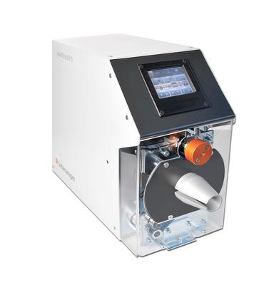
New Equipment | Cable & Wire Harness Equipment
Overview The JacketStrip 8310 axially and radially slits the insulation of out-of-round and multi-conductor cables from 2.5 - 25 mm (0.1" - 1'') O.D. and up to 500 mm (19.7") in stripping length without any damage to the inner conductors or shieldin
Industry News | 2017-01-05 04:27:37.0
BGA Inspection & Defect Photo Album (Can be downloaded) The photo CD-ROM album featuring over 280 colour images on BGA, materials, inspection and defects and is available to allow engineers to create their own training material, PowerPoint files, process documents, technical articles and standards. The disk includes examples of the following:

The JacketStrip 8310 axially and radially slits the insulation of out-of-round and multi-conductor cables from 0.1" - 1'' (2.5 - 25 mm) O.D. and up to 19.7" (500 mm) in stripping length without any damage to the inner conductors or shielding.
Industry Directory | Manufacturer
Buyers of Scrap Materials and Surplus Machinery, Equipment and Inventories Precious Metal Refining Warehouse Liquidation PCB & Electronic Scrap Recycling Purchasing of Used Surplus Semiconductor
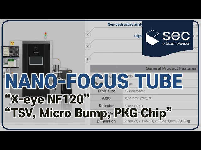
#Xray#Inspection#SEC Nano-focus Tube of 200 nano resolution which is specialized for sub-micron defects of Semiconductor Packaging, Wafer Level Packaging(WLP). -Non-destructive Analysis System -High-Resolution Image with Dual Type CTs -Application


