Industry News | 2019-11-05 22:08:21.0
Via in pad is the design practice of placing a via in the copper landing pad of a component. Compared to standard PCB via routing, via in pad allows a design to use smaller component pitch sizes and further reduce the PCBs overall size. With component manufactures pushing smaller parts every year and the demand from consumers for smaller devices, the usage of via in pad practices by hardware engineers have become more commonplace. In this article, we will discuss the differences between via in pad and traditional vias, when should you use via in pad, and how to design for it.
Technical Library | 2016-03-03 17:25:26.0
This paper discusses a nano copper based paste for use in via filling. The company manufactures nano copper and disperses the coated nano copper into a paste in combination with micron copper. The resultant paste is injected or fills a via. The via is subsequently sintered by means of photonic sintering, or by heat in a reducing environment. The process will be accomplished in under an hour and results in filled solid copper vias.
New Equipment | Coating Materials
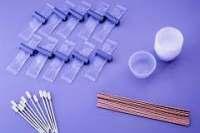
This kit contains 10 packages of clear, low viscosity, superior strength epoxy, precisely measured out into two-compartment plastic packages so it's easy to use and there's no measuring. Once cured, this epoxy makes an effective electrical insulator
Technical Library | 2019-06-26 23:21:49.0
Copper-filled micro-vias are a key technology in high density interconnect (HDI) designs that have enabled increasing miniaturization and densification of printed circuit boards for the next generation of electronic products. Compared with standard plated through holes (PTHs) copper filled vias provide greater design flexibility, improved signal performance, and can potentially help reduce layer count, thus reducing cost. Considering these advantages, there are strong incentives to optimize the via filling process. This paper presents an innovative DC acid copper via fill formulation, for VCP (Vertical Continues Plating) applications which rapidly fills vias while minimizing surface plating.
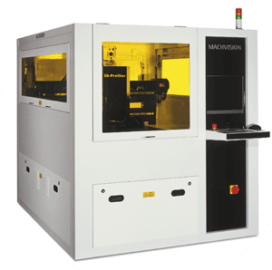
The 3D Profiler is an automatic machine to measure the dent of the copper filled vias. The system offers the opportunity for 100% inspection to ensure the yield of the copper filling with inspection speeds of 5 minutes per panel and +/- 2 micron accu
Industry Directory | Manufacturer
Suppliers of adhesive and dispensing solutions. Techcon dispensers, metering valves, robots, plastic components, air guns and accessories. Henkel Sicomet anaerobic and cyanoacrylate adhesives, Henkel Dexter epoxy resins and adhesives, Jenome dispensing robots. Keltech pressure pot dispensers. Packaging service for transfer of adhesives from drums, pots or cans into syringes and cartridges.
Technical Library | 2021-05-26 00:53:26.0
This paper describes a copper electroplating enabling technology for filling microvias. Driven by the need for faster, smaller and higher performance communication and electronic devices, build-up technology incorporating microvias has emerged as a viable multilayer printed circuit manufacturing technology. Increased wiring density, reduced line widths, smaller through-holes and microvias are all attributes of these High Density Interconnect (HDI) packages. Filling the microvias with conductive material allows the use of stacked vias and via in pad designs thereby facilitating additional packaging density. Other potential design attributes include thermal management enhancement and benefits for high frequency circuitry. Electrodeposited copper can be utilized for filling microvias and provides potential advantages over alternative via plugging techniques. The features, development, scale up and results of direct current (DC) and periodic pulse reverse (PPR) acid copper via filling processes, including chemistry and equipment, are described.
Technical Library | 2019-10-10 00:26:28.0
Voids are a plague to our electronics and must be eliminated! Over the last few years we have studied voiding in solder joints and published three technical papers on methods to "Fill the Void." This paper is part four of this series. The focus of this work is to mitigate voids for via in pad circuit board designs. Via holes in Quad Flat No-Lead (QFN) thermal pads create voiding issues. Gasses can come out of via holes and rise into the solder joint creating voids. Solder can also flow down into the via holes creating gaps in the solder joint. One method of preventing this is via plugging. Via holes can be plugged, capped, or left open. These via plugging options were compared and contrasted to each other with respect to voiding. Another method of minimizing voiding is through solder paste stencil design. Solder paste can be printed around the via holes with gas escape routes. This prevents gasses from via holes from being trapped in the solder joint. Several stencil designs were tested and voiding performance compared and contrasted. In many cases voiding will be reduced only if a combination of mitigation strategies are used. Recommendations for combinations of via hole plugging and stencil design are given. The aim of this paper is to help the reader to "Fill the Void."
Technical Library | 2022-01-26 15:26:56.0
In this work an attempt is made to improve the fracture toughness and electrical conductivity of epoxy/glass fiber based laminates by the inclusion of carbon nanotube (CNT) fillers. The fiber orientation of the epoxy/ glass fiber (GF) fabric laminates was optimized based on estimation of mechanical properties. The carboxylic acid functionalized CNTs were incorporated into epoxy matrix by ultra-sonication method. The nano filled epoxy resin was used to prepare laminates with 30/45 GF fabric orientation. The CNT content was varied and its effect on the tensile properties was determined. The fracture toughness of multiphase composites was estimated using single edge notch bend (SENB) test. The presence of CNTs improved the fracture toughness by a crack bridging mechanism. The volume resistivity of multiphase composites was found to be superior to the conventional epoxy/CNT composite. The presence of glass fabric reduces the number of inter-tube contacts contributing to the reduction in volume resistivity.
Training Courses | | | IPC-7711/7721 Specialist (CIS)
The Certified IPC-7711/7721 Specialist (CIS) training focuses on rework of electronic assemblies and repair and modification of printed boards and electronic assemblies.


