Industry News | 2020-10-04 15:41:30.0
MacDermid Alpha Electronics Solutions will be exhibiting at the Taiwan Printed Circuit Association (TPCA) exhibition and presenting two technical papers at the IMPACT-EMAP Conference, co-located with TPCA in Taipei, October 21-23, 2020. The papers detail some of the ways in which MacDermid Alpha has invested in the research of innovative manufacturing processes to meet the demanding standards required for the new age of miniaturization.
Industry News | 2023-11-13 12:22:31.0
Ventec Giga Solutions, the equipment division of Ventec International Group announces its appointment by Sunus Precision Machinery as sales agent and distributor of Vacuum Filling Holes Solutions and Screen Printing Equipment. The agreement covers all regions globally outside of Asia.
Industry Directory | Consultant / Service Provider / Manufacturer
Manufacturer of highly miniaturized and high reliability PCBs. Swiss Quality substrates for demanding applications such as implants and medical devices. HDI flex, rigid-flex and rigid PCBs in small to medium volumes.
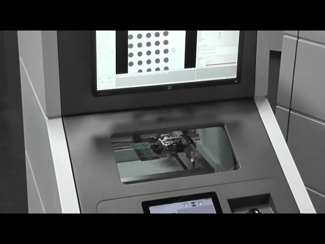
Semi-automated, programmable X-ray inspection system with multi-axis for prototyping, failure analysis, manufacturing process validation and rework verification for PCBs up to 18 x 20". The XT-3 is a high quality high-resolution manual x-ray inspecti
Technical Library | 2008-08-28 22:50:11.0
The increasing use of lead-free solder has introduced a new set of process parameters when setting up wave solder equipment for effective soldering. Determining the proper flow characteristics of the solder wave for adequate hole fill is an essential step in achieving a reliable process. A variety of solder waves exist in the industry; each with advantages and disadvantages when performing lead-free wave soldering. One way to ensure adequate hole-fill is by increasing contact time at the Chip Wave.
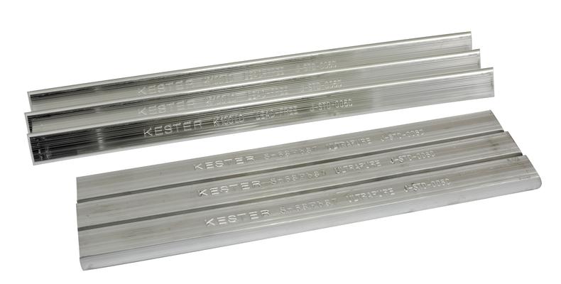
New Equipment | Solder Materials
Manufactured by a special process that controls the inclusions of oxides and metallic and non-metallic impurities, Kester Ultrapure® is the industry standard bar solder for use in high tech electronic applications where lower surface tension and hole
Technical Library | 2024-05-16 16:06:24.0
Much like actual cities where streets and roads connect buildings together, ICs on a board are connected to each other with copper traces. And just like any metropolitan city, urban expansion tends to move vertically instead of horizontally, but instead of multi-story buildings, we get multilayer boards. Vias are copper-plated holes spanning through the different layers of a given board or panel. They are the entrance locations to the subway stations, if you will. Having those multilayer boards has enabled electronic design to minimize the size of boards immensely without compromising on the complexity.
New Equipment | Solder Paste Stencils
Through the increase of mixed technologies, stepped stencils have gained importance to the electronic assembly manufacturer. If the solder paste quantity can no longer be adequately regulated by adjusting Step/Relief Stencil Picture the pad sizes, st
Industry News | 2011-04-06 13:13:52.0
Dow Electronic Materials will showcase its innovative materials for printed circuit boards (PCBs) at this year’s IPC APEX EXPO. Dow will feature a number of its latest products that are tailored to meet the requirements of increasingly complex circuit boards while delivering ever-higher reliability and consistency. Dow’s next-generation of high quality, cost-effective technologies allow customers to meet future market requirements.


