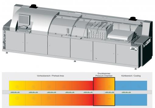
Innovative technology for virtually void-free reflow soldering processes. Particularly suited for demanding applications. Whether for power electronics, electronic aviation systems, medical equipment or electronic systems for the automotive industr
Industry News | 2010-09-08 11:49:17.0
PCB Fabricator Installs MASS VHF 300 VS for Via Hole Filling Addressing the continuous demands pertaining to via hole filling, through holes and blind vias
Industry News | 2010-11-09 10:15:49.0
With IPC-4761 as its guide, PCB Manufacturer sheds light on Via Plugging from the fabrication perspective.
Technical Library | 2021-05-26 00:53:26.0
This paper describes a copper electroplating enabling technology for filling microvias. Driven by the need for faster, smaller and higher performance communication and electronic devices, build-up technology incorporating microvias has emerged as a viable multilayer printed circuit manufacturing technology. Increased wiring density, reduced line widths, smaller through-holes and microvias are all attributes of these High Density Interconnect (HDI) packages. Filling the microvias with conductive material allows the use of stacked vias and via in pad designs thereby facilitating additional packaging density. Other potential design attributes include thermal management enhancement and benefits for high frequency circuitry. Electrodeposited copper can be utilized for filling microvias and provides potential advantages over alternative via plugging techniques. The features, development, scale up and results of direct current (DC) and periodic pulse reverse (PPR) acid copper via filling processes, including chemistry and equipment, are described.
40mm Applications Solder Joint Quality (BGA, Leaded) Bridging Voiding Opens Bare boards (Inner layers, traces, vias) Component Package Inspection (wire bonds) Subtle Defect Inspection
Industry Directory | Manufacturer
PCB Repairs of all kinds including-Solder on Tab (Solder Removal, Gold Plating), PTH & Delam repairs, etc.
Technical Library | 2014-11-13 19:23:50.0
With increasing power loss of electrical components, thermal performance of an assembled device becomes one of the most important quality factors in electronic packaging. Due to the rapid advances in semiconductor technology, particularly in the regime of high-power components, the temperature dependence of the long-term reliability is a critical parameter and has to be considered with highest possible care during the design phase (...) The aim of this paper is to give a short overview about standard thermal solutions like thick copper, thermal vias, plugged vias or metal core based PCBs. Furthermore, attention will be turned on the development of copper filled thermal vias in thin board constructions...

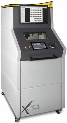
Wafer-level Product In-line(Ireland) 2D, 3D CT AXI Machine Automatic inspection equipment exclusively for the Wafer-level products and ultra-fine defects of mm can be detected using the Nano Tube of Class Focal spot 200nm. 2D, as well as 70&o
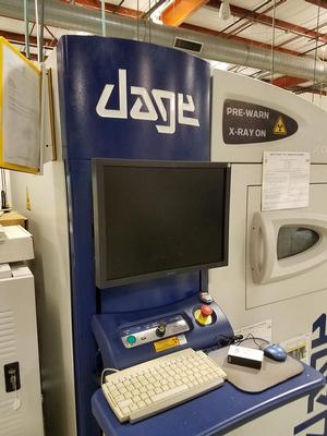
Used SMT Equipment | X-Ray Inspection
Dage X Ray Inspection Machine Model: XD7500 Year: 2004 S/N: X23484 Dage NT950 "sealed transmissive", "filament-free" X ray tube *NEEDS REPLACEMENT Includes: • Lead-shielded system safety cabinet with lead-glass view window in sample door (X-r
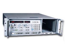
Used SMT Equipment | In-Circuit Testers
Agilent-Keysight 8350B The totally programmable features and internal memory of the 8350B Sweep Oscillator Mainframe can speed up your repetitious testing needs. A push of a button returns the unit to local control for bench work. Sweep frequency


