Technical Library | 2019-08-07 22:56:45.0
The requirement to reconsider traditional soldering methods is becoming more relevant as the demand for bottom terminated components (QFN/BTC) increases. Thermal pads under said components are designed to enhance the thermal and electrical performance of the component and ultimately allow the component to run more efficiently. Additionally, low voiding is important in decreasing the current path of the circuit to maximize high speed and RF performances. The demand to develop smaller, more reliable, packages has seen voiding requirements decrease below 15 percent and in some instances, below 10 percent.Earlier work has demonstrated the use of micro-fluxed solder preforms as a mechanism to reduce voiding. The current work builds upon these results to focus on developing an engineered approach to void reduction in leadless components (QFN) through increasing understanding of how processing parameters and a use of custom designed micro-fluxed preforms interact. Leveraging the use of a micro-fluxed solder preform in conjunction with low voiding solder paste, stencil design, and application knowhow are critical factors in determining voiding in QFN packages. The study presented seeks to understand the vectors that can contribute to voiding such as PCB pad finish, reflow profile, reflow atmosphere, via configuration, and ultimately solder design.A collaboration between three companies consisting of solder materials supplier, a power semiconductor supplier, and an electronic assembly manufacturer worked together for an in-depth study into the effectiveness of solder preforms at reducing voiding under some of the most prevalent bottom terminated components packages. The effects of factors such as thermal pad size, finish on PCB, preform types, stencil design, reflow profile and atmosphere, have been evaluated using lead-free SAC305 low voiding solder paste and micro-fluxed preforms. Design and manufacturing rules developed from this work will be discussed.
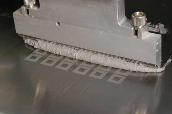
Technical Library | 2020-12-29 20:55:46.0
Voiding in solder joints has been studied extensively, and the effects of many variables compared and contrasted with respect to voiding performance. Solder paste flux, solder powder size, stencil design, circuit board design, via-in-pad design, surface finish, component size, reflow profile, vacuum reflow, nitrogen reflow and other parameters have been varied and voiding quantified for each. The results show some differences in voiding performance with respect to most of these variables but these variables are not independent of each other. Voiding in solder joints is a complex issue that often requires multiple approaches to reduce voiding below required limits. This paper focuses on solutions to voiding for commonly used bottom terminated components (BTCs).
Technical Library | 2018-10-03 20:41:44.0
Voids in solder joints plague many electronics manufacturers. Do you have voids in your life? We have good news for you, there are many excellent ways to "Fill the Void." This paper is a continuation of previous work on voiding in which the following variables were studied: water soluble lead-free solder pastes, a variety of stencil designs, and reflow profiles. Quad Flat No-Lead (QFN) component thermal pads were used as the test vehicle. The voiding results were summarized and recommendations were made for reduction of voiding.
Industry News | 2016-10-13 15:46:28.0
KIC today announced plans to exhibit at the New England Expo & Tech Forum, scheduled to take place Thursday, November 3, 2016 at the DCU Center in Worcester, MA. MB (Marybeth) Allen will present “Optimization of the Reflow Profile to Minimize Voiding.”
Industry News | 2016-10-17 18:55:57.0
KIC today announced plans to exhibit at the SMTA Space Coast Expo & Tech Forum, scheduled to take place Thursday, Nov. 17, 2016 at the Melbourne Auditorium in FL. MB (Marybeth) Allen will present “Optimization of the Reflow Profile to Minimize Voiding” at 11 a.m.
Industry News | 2019-01-08 20:21:17.0
KIC and Indium Corporation will hold a voiding clinic in Booth #1215 at the 2019 IPC APEX EXPO, scheduled to take place Jan. 29-31 at the San Diego Convention Center.
Technical Library | 2007-04-04 11:43:41.0
The present work offers a discussion and a first case study to identify and illustrate voiding mechanisms for a particular TIM between a heat spreader and the back of a flip chip. Pronounced differences were observed between stencil printing and dispensing in terms of initial void formation, apparently related to the specific properties of the material. Measurements of the effects of heat ramp rate and peak temperature showed the subsequent evolution and final void size distribution to be determined by the initial part of the cure profile up to the material gelling temperature.
Technical Library | 2017-11-15 22:49:14.0
While a significant level of voiding can be tolerated in solder joints where electrical conductivity is the main requirement, voiding at any level severely compromises thermal conductivity. For example, in LED lighting modules effective conduction of heat through the 1st level die attach to the substrate and then through the 2nd level attach to the heat sink is critical to performance so that voiding in the solder joints at both levels must be minimized. (...) In this paper, the authors will review the factors that influence the incidence of voids in small and large area solder joints that simulate, respectively, the 1st and 2nd level joints in LED modules and discuss mitigation strategies appropriate to each level. They will also report the results of a study on the effect on the incidence of voids of flux medium formulation and the optimization of the thermal profile to ensure that most of the volatiles are released early in the reflow process.
New Equipment | Solder Materials
Indium Corporation manufactures high quality solder powders and pastes. Powders are available in hundreds of alloys and a full range of sizes. Solder pastes can be made from these powders using a wide variety of flux vehicles to get the best fit for
Industry News | 2016-09-01 19:24:28.0
KIC today announced that Marybeth (MB) Allen will present “Optimized Reflow Profiling to Minimize Voiding” during SMTA International. The presentation is scheduled to take place during the IPC Session ‘Lead-Free Symposium,’ Session LF2 on Thursday, Sept. 29, 2016 from 11 a.m.-12 p.m.


