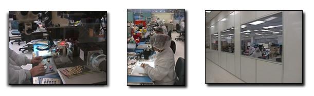
PROMEX INDUSTRIES now fills the need for on shore integrated circuit assembly and packaging foundry services for small lots and prototypes through medium volume production. We are committed to providing high quality, quick turnaround semiconductor
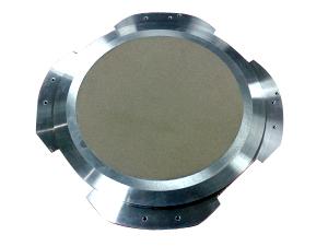
Porous ceramic vacuum chuck table or Polishing Chuck table supplied to semiconductor industry for silicon wafer dicing or finishing purposes. This product is an uniform compact frame, high strength, good porosity, durable absorption, excellent quali
To compliment our wafer dicing and inspection processes, Syagrus Systems offers fully automated die sorting services. Whether you require high volume production or a single wafer prototype build, Syagrus Systems has the die sorting solution for you.
Majelac Technologies provides subcontract assembly services to the semiconductor & optoelectronic industries. We specialize in Quick Turn Assembly & Packaging of Ball Grid Array packages and can handle a large variety of other package types.�Majela
Syagrus Systems uses the 3M Wafer Support System to meet the demands of today's technology companies for extremely thin silicon wafers and die used in complex applications. We have over 15 years of silicon wafer thinning and wafer backgrinding experi
Industry Directory | Equipment Dealer / Broker / Auctions
Trading of Used Electronics and Semiconductor Machines and Equipment
Majelac Technologies provides subcontract assembly services to the semiconductor & optoelectronic industries. We specialize in Quick Turn Assembly & Packaging of Ball Grid Array packages and can handle a large variety of other package types.�Majela
NEPTCO�s WAFERTAPE family of products for wafer mounting, dicing and backgrinding is designed to insure consistent, precise, and repeatable wafer production yields. NEPTCO's superior coating technology encompasses Total Thickness Variation (TTV) co

Syagrus Systems has a long history in providing superior wafer and die visual inspection services to the semiconductor industry. Syagrus Systems features fully automated wafer inspection systems as well as the flexibility of manual wafer inspection
Career Center | San Jose, California USA | Engineering,Research and Development
Advanced Packaging Engineer � Develop advanced packaging technologies and processes, including: wafer thinning and dicing; die attach; wire bonding; overmolding; singulation � Perform Design of Experiments to establish optimized process windows for


