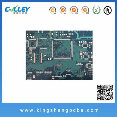
New Equipment | Fabrication Services
Our Service PCB Assembly and PCB&PCBA design are our main business.We are able to undertake a high quality Printed Circuit Board Assembly on competitive prices and flexible conditions.We are a complete “One- Stop” resource for printed circuit board
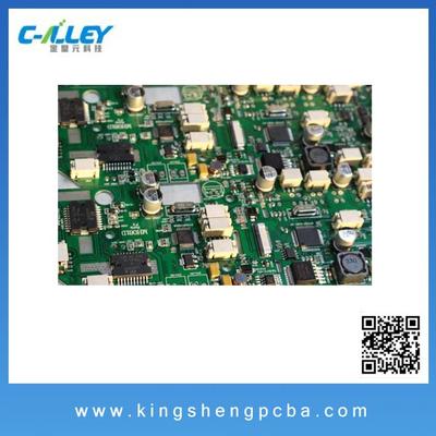
New Equipment | Assembly Services
Our Service PCB Assembly and PCB&PCBA design are our main business.We are able to undertake a high quality Printed Circuit Board Assembly on competitive prices and flexible conditions.We are a complete “One- Stop” resource for printed circuit board
Electronics Forum | Mon Jun 03 12:51:17 EDT 2002 | V.RAMANAND KINI
We are doing COB operations for nearly ten years. Pls. write to me if you need info on m/c selection, type of PCB, plating etc., Thanks V.RAMANAND KINI...03.06.02
Electronics Forum | Mon May 07 11:02:17 EDT 2001 | Singh
Hi all. I am looking into the implementation of the Chip on Board process with eutactic bonding and the then using either gold or aluminum wire to make wedge type wire bonding. Since I am totally new to this, can somebody guide me thru the process,
Industry News | 2015-06-11 16:02:18.0
MIRTEC, "The Global Leader in Inspection Technology," will exhibit its most recent solutions for System in Package (SiP) inspection and measurement at SEMICON WEST 2015; July 14-16, 2015, at the Moscone Center in San Francisco, CA. Visitors are invited to booth # 2343 for a detailed demonstration of this exciting new technology.
Industry News | 2012-01-23 00:02:12.0
MIRTEC, “The Global Leader in Inspection Technology”, will premier its complete line of 3D AOI, SPI, X-ray and LED inspection systems at the IPC APEX Expo in booth #3637.
Technical Library | 2011-03-30 21:14:33.0
The expression "multifunctional PCB", as a synonym for a PCB which is applicable with a variety of assembly techniques, is already established on the market. That means the PCB can be used for multiple reflow soldering and multiple assembly techniques lik
Technical Library | 2020-08-27 01:22:45.0
Initially adopted internal specifications for acceptance of printed circuit boards (PCBs) used for wire bonding was that there were no nodules or scratches allowed on the wirebond pads when inspected under 20X magnification. The nodules and scratches were not defined by measurable dimensions and were considered to be unacceptable if there was any sign of a visual blemish on wire-bondable features. Analysis of the yield at a PCB manufacturer monitored monthly for over two years indicated that the target yield could not be achieved, and the main reasons for yield loss were due to nodules and scratches on the wirebonding pads. The PCB manufacturer attempted to eliminate nodules and scratches. First, a light-scrubbing step was added after electroless copper plating to remove any co-deposited fine particles that acted as a seed for nodules at the time of copper plating. Then, the electrolytic copper plating tank was emptied, fully cleaned, and filtered to eliminate the possibility of co-deposited particles in the electroplating process. Both actions greatly reduced the density of the nodules but did not fully eliminate them. Even though there was only one nodule on any wire-bonding pad, the board was still considered a reject. To reduce scratches on wirebonding pads, the PCB manufacturer utilized foam trays after routing the boards so that they did not make direct contact with other boards. This action significantly reduced the scratches on wire-bonding pads, even though some isolated scratches still appeared from time to time, which caused the boards to be rejected. Even with these significant improvements, the target yield remained unachievable. Another approach was then taken to consider if wire bonding could be successfully performed over nodules and scratches and if there was a dimensional threshold where wire bonding could be successful. A gold ball bonding process called either stand-off-stitch bonding (SSB) or ball-stitch-on-ball bonding (BSOB) was used to determine the effects of nodules and scratches on wire bonds. The dimension of nodules, including height, and the size of scratches, including width, were measured before wire bonding. Wire bonding was then performed directly on various sizes of nodules and scratches on the bonding pad, and the evaluation of wire bonds was conducted using wire pull tests before and after reliability testing. Based on the results of the wire-bonding evaluation, the internal specification for nodules and scratches for wirebondable PCBs was modified to allow nodules and scratches with a certain height and a width limitation compared to initially adopted internal specifications of no nodules and no scratches. Such an approach resulted in improved yield at the PCB manufacturer.
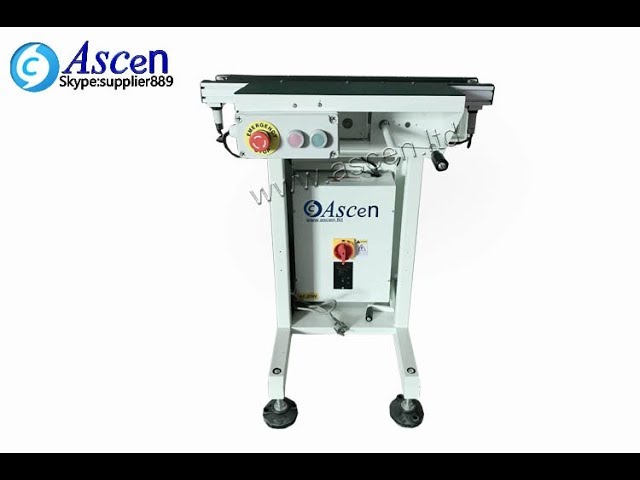
https://www.ascen.ltd/Products/Automatic_SMT_equipment/PCB_conveyor/100.html PCB linking conveyor and PCB belt conveyor mainly used to connect different type PCB board handing equipment effectively for the SMT production line. ASCEN technology is ava
https://www.ascen.ltd/Products/Automatic_SMT_equipment/PCB_conveyor/100.html PCB linking conveyor and PCB belt conveyor mainly used to connect different type PCB board handing equipment effectively for the SMT production line. ASCEN technology is ava
Gold Wire Bonding Performance and Reliability of ENEPIG Surface Finishes Gold Wire Bonding Performance and Reliability of ENEPIG Surface Finishes The expression "multifunctional PCB", as a synonym for a PCB which is applicable with a variety
GPD Global | https://www.gpd-global.com/pdf/doc/Kits-and-Parts-for-Dispensers-and-Related-Equipment-22290036.pdf
cleaning wire kits detail.1 32 4 5 6 CLEANING WIRE KITS Each kit/set includes 4 tapered-tip wires and 3 scoop-end drill bits for a single gauge. 18 gauge = 10/4311 20 gauge = 10/3720 21 gauge = 10/3721 22 gauge = 10/3722 23 gauge = 10/3723 25 gauge = 10/3725
Imagineering, Inc. | https://www.pcbnet.com/blog/the-role-of-pcb-assembly-and-fabrication-in-the-aerospace-industry/
) and an in-plane CTE of about 15 ppm/°C. These thermal properties resemble ceramic-bodied microcircuits that manufacturers typically solder to a PCB

Products, services, training & consulting for the assembly, rework & repair of electronic assemblies. BGA process experts. Manufacturers Rep, Distributor & Service Provider for Seamark/Zhuomao and Shuttle Star BGA Rework Stations.
Training Provider / Manufacturer's Representative / Equipment Dealer / Broker / Auctions / Consultant / Service Provider
1750 Mitchell Ave.
Oroville, CA USA
Phone: (888) 406-2830


