Electronics Forum | Wed Jan 09 21:19:49 EST 2002 | davef
When I said "In this area, there is no difference between your experience in ceramic substrates and PTFE substrates." I was referring to the area we were discussing ... gold plating. I am sorry if you thought I ment than the wire bonding process wa
Electronics Forum | Mon Jan 07 20:37:15 EST 2002 | davef
For soldered areas, we like to keep gold thickness substantially below the maximum you propose. Search the fine SMTnet Archives for our discussions on the topic of acceptable levels of gold with solder connections. Let�s fix this �no one seems be s
Industry News | 2018-12-08 03:29:29.0
SMT Dictionary – Surface Mount Technology Acronym and Abbreviation
Industry News | 2012-09-10 09:15:27.0
MARTIN will be one of nine companies participating in the Package on Package Design and Assembly Center (PoP Center) at SMTA International this year.
Technical Library | 2020-08-27 01:22:45.0
Initially adopted internal specifications for acceptance of printed circuit boards (PCBs) used for wire bonding was that there were no nodules or scratches allowed on the wirebond pads when inspected under 20X magnification. The nodules and scratches were not defined by measurable dimensions and were considered to be unacceptable if there was any sign of a visual blemish on wire-bondable features. Analysis of the yield at a PCB manufacturer monitored monthly for over two years indicated that the target yield could not be achieved, and the main reasons for yield loss were due to nodules and scratches on the wirebonding pads. The PCB manufacturer attempted to eliminate nodules and scratches. First, a light-scrubbing step was added after electroless copper plating to remove any co-deposited fine particles that acted as a seed for nodules at the time of copper plating. Then, the electrolytic copper plating tank was emptied, fully cleaned, and filtered to eliminate the possibility of co-deposited particles in the electroplating process. Both actions greatly reduced the density of the nodules but did not fully eliminate them. Even though there was only one nodule on any wire-bonding pad, the board was still considered a reject. To reduce scratches on wirebonding pads, the PCB manufacturer utilized foam trays after routing the boards so that they did not make direct contact with other boards. This action significantly reduced the scratches on wire-bonding pads, even though some isolated scratches still appeared from time to time, which caused the boards to be rejected. Even with these significant improvements, the target yield remained unachievable. Another approach was then taken to consider if wire bonding could be successfully performed over nodules and scratches and if there was a dimensional threshold where wire bonding could be successful. A gold ball bonding process called either stand-off-stitch bonding (SSB) or ball-stitch-on-ball bonding (BSOB) was used to determine the effects of nodules and scratches on wire bonds. The dimension of nodules, including height, and the size of scratches, including width, were measured before wire bonding. Wire bonding was then performed directly on various sizes of nodules and scratches on the bonding pad, and the evaluation of wire bonds was conducted using wire pull tests before and after reliability testing. Based on the results of the wire-bonding evaluation, the internal specification for nodules and scratches for wirebondable PCBs was modified to allow nodules and scratches with a certain height and a width limitation compared to initially adopted internal specifications of no nodules and no scratches. Such an approach resulted in improved yield at the PCB manufacturer.
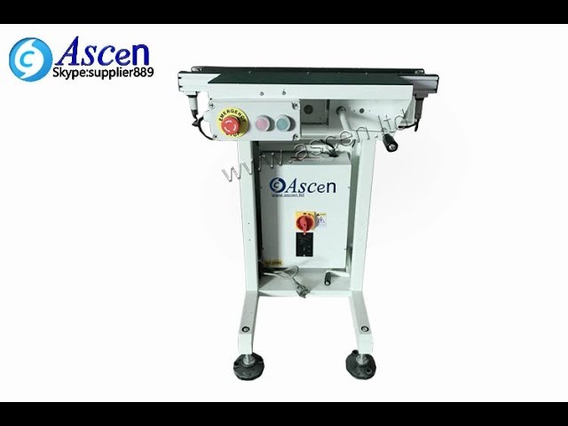
https://www.ascen.ltd/Products/Automatic_SMT_equipment/PCB_conveyor/100.html PCB linking conveyor and PCB belt conveyor mainly used to connect different type PCB board handing equipment effectively for the SMT production line. ASCEN technology is ava
https://www.ascen.ltd/Products/Automatic_SMT_equipment/PCB_conveyor/100.html PCB linking conveyor and PCB belt conveyor mainly used to connect different type PCB board handing equipment effectively for the SMT production line. ASCEN technology is ava
Gold Wire Bonding Performance and Reliability of ENEPIG Surface Finishes Gold Wire Bonding Performance and Reliability of ENEPIG Surface Finishes The expression "multifunctional PCB", as a synonym for a PCB which is applicable with a variety
ASYMTEK Products | Nordson Electronics Solutions | https://www.nordson.com/en/divisions/march/process/etchback-and-desmear?con=t&page=10
Fluorine, Organic and Metal Oxide Contamination for Improved Wire Bonding Performance Nordson MARCH Technology Drivers for Plasma Prior to Wire Bonding Nordson MARCH Plasma Power Plus Nordson MARCH Our
Imagineering, Inc. | https://www.pcbnet.com/blog/the-role-of-pcb-assembly-and-fabrication-in-the-aerospace-industry/
. In addition to protecting wiring from corrosion, these coatings must be highly heat-resistant. PCB Assembly in Aerospace PCB assembly for aerospace applications is the process of building and testing circuits on a PCB in an aerospace environment to ensure it works as intended

Products, services, training & consulting for the assembly, rework & repair of electronic assemblies. BGA process experts. Manufacturers Rep, Distributor & Service Provider for Seamark/Zhuomao and Shuttle Star BGA Rework Stations.
Training Provider / Manufacturer's Representative / Equipment Dealer / Broker / Auctions / Consultant / Service Provider
1750 Mitchell Ave.
Oroville, CA USA
Phone: (888) 406-2830


