Industry News | 2015-05-07 19:28:29.0
MIRTEC announce a new strategic cooperation that will empower yield improvement in the electronics manufacturing industry.
Industry News | 2015-06-11 16:02:18.0
MIRTEC, "The Global Leader in Inspection Technology," will exhibit its most recent solutions for System in Package (SiP) inspection and measurement at SEMICON WEST 2015; July 14-16, 2015, at the Moscone Center in San Francisco, CA. Visitors are invited to booth # 2343 for a detailed demonstration of this exciting new technology.
Industry News | 2013-05-01 12:45:51.0
Held at the Rijckholt Castle and Nordson ASYMTEK European Headquarters in Maastricht
Industry News | 2011-01-12 17:40:04.0
Check out these Show Highlights, Ways to Save, Networking and Educational Opportunities, and Exhibition Preview.
Industry News | 2023-05-15 17:38:25.0
IPC and the International Microelectronics Assembly and Packaging Society (IMAPS) will host an "On-Shoring Advanced Packaging and Assembly," workshop July 10-12, 2023, in Washington, D.C.
Industry News | 2024-03-11 15:00:03.0
Connect with our experts and see plasma and dispensing equipment for microelectronics manufacturing in booth 3645
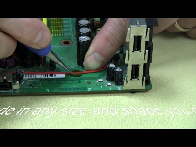
This video demonstrated the use of BEST Inc HotDots(TM) which allow wires to be affixed to the PCB or other surfaces-even when those surfaces go through reflow. There are other similar products out there but none of which can be readily customized no
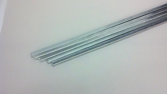
New Equipment | Solder Materials
GalvRepair the structural steel sndustry standard for galvanizing repair for almost 60 years. Kapp GalvRepair solder is the leading formulation designed specifically for high quality repairs to galvanized steel surfaces. GalvRepair is simple, effecti
Technical Library | 2014-05-08 16:34:16.0
Bare die mounting on multi-device substrates has been in use in the microelectronics industry since the 1960s. The aerospace industry’s hybrid modules and IBM’s Solid Logic Technology were early implementations that were developed in the 1960’s. The technologies progressed on a steady level until the mid 1990’s when, with the advent of BGA packaging and chip scale packages, the microelectronics industry started a wholesale move to area array packaging. This paper outlines the challenges for both traditional wire-bond die attached to a printed wiring board (pwb), to the more recent applications of bumped die attached to a high performance substrate.
Industry News | 2015-06-18 17:55:13.0
Indium Corporation and the Empire Chapter of the International Microelectronics Assembly and Packaging Society (IMAPS), in association with the State University of New York (SUNY), will host an Advanced Technology Workshop and Tabletop Exhibition on Advances in Semiconductor Packaging on Sept. 24 at SUNY Polytechnic Institute in Marcy, N.Y.


