Events Calendar | Wed Jun 20 00:00:00 EDT 2018 - Wed Jun 20 00:00:00 EDT 2018 | ,
Everything You Need to Know About X-Rays
Training Courses | | | PCB Assembly Courses
The PCB assembly courses provide knowledge of different processes and equipment used in TH and SMT assembly of printed circuit boards.
Technical Library | 2023-11-20 17:30:11.0
Summary for today 1. Electronic component inspection and failure analysis. 2. Component counting and material management. 3. Reverse engineering. 4. Counterfeit detection. 5. Real-time defect verification. 6. Computed tomography (CT) techniques and how to differentiate between 2D, 2.5D, and 3D x-ray inspection. 7. Design for manufacturing (DFM) and design for x-ray inspection (DFXI). 8. Voids, bridging, and head-in-pillow failures in bottom terminated components (BTC). 9. Artificial Intelligence and x-ray inspection
Industry Directory | Manufacturer
ITS (www.itechserv.com) provides a full range of electronics manufacturing, test, logistics and repair services. Fine pitch SMT, ICT, HASS, box build, BGA repair, X-Ray and is ISO9001. Real time lot tracibility and serial data collection system RTM 3
Gary Ellenbogen, D.D.S. is a general and cosmetic dentist who has been providing excellent dental services to patients throughout the Fairfax County, Virginia area for over 34 years.
Industry Directory | Manufacturer
Adonai Technologies is a full service EMS company, specializing in Class 3 manufacturing. We provide quick turn prototyping and any size production runs. Capabilities include x-ray, conformal coating and functional test.
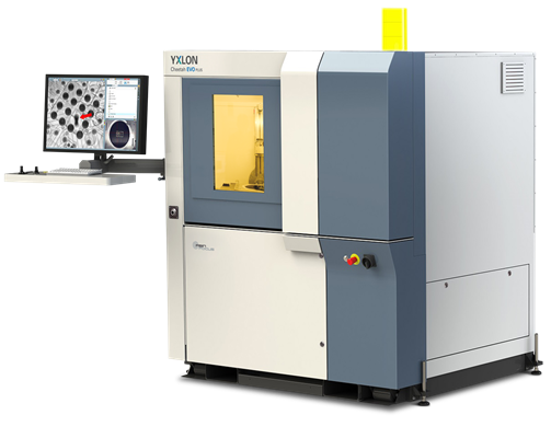
The YXLON Cheetah EVO series was designed to provide the "best-in-class" inspection solution for SMT, semiconductor, and laboratory assembly applications. With optimitzed software and hardware, these systems produce higher quality and more consistent
Events Calendar | Tue Jan 23 00:00:00 EST 2018 - Tue Jan 23 00:00:00 EST 2018 | Fremont, California USA
Digital X-Ray Inspection Services Open House
Industry News | 2001-06-05 05:33:07.0
phoenix|x-ray Systems + Services recently completed the development of a nanofocus X-ray tube. This new tube technology provides a 500 nanometers (0.5 microns) lateral resolution for phoenix|x-ray X-ray systems, which is a remarkable step, migrating the company's products into the submicron region.
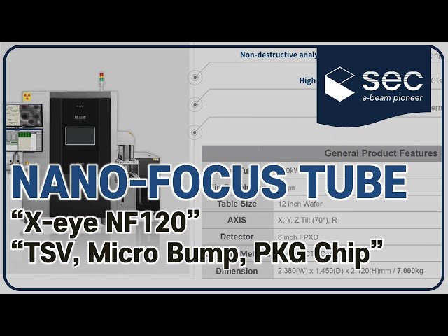
#Xray#Inspection#SEC Nano-focus Tube of 200 nano resolution which is specialized for sub-micron defects of Semiconductor Packaging, Wafer Level Packaging(WLP). -Non-destructive Analysis System -High-Resolution Image with Dual Type CTs -Application


