New Equipment | Rework & Repair Equipment
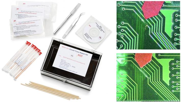
The BEST PCB circuit trace repair kit gives you the tools you need for fast modification and repair of PCB circuit traces. Our online PCB repair training videos, our master instructors along with these materials allows you to meet the original PCB qu
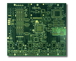
8 layers board Basic Material: FR-4 Board Ply (thickness): 1.80mm Measurement: 254mm x 304.8mm Conductor Width: 5mil (0.13mm) Conductor Spacing: 5mil (0.13mm) Surface Treatment: Immersion gold File Format: Gerber File (RS274X) Through Hole: 2
Layer Count: 2L Board Thickness: 0.8mm Dimension: 140*85mm Material: Rogers RO5880 Surface Copper: 35μm Min Hole Diameter: 2.0mm Min line Width/Space: N/A Surface Finish: ENIG Do you need a PCB for special signal requirement into your products? High
At Barry: custom requests are common and welcome. We enjoy the challange. Extensive capabilities, wide material selection and state-of-the-art equiptment (including in-house plating and machining) ensure we can deliver a component fitting your exact
Parmod�, Parelec Inc�s patented conductive ink technology, enables the formation of continuous-phase pure metallic conductors at relatively low temperature�making them suitable for application to polymer substrates. Parmod� inks, pastes and toners ca
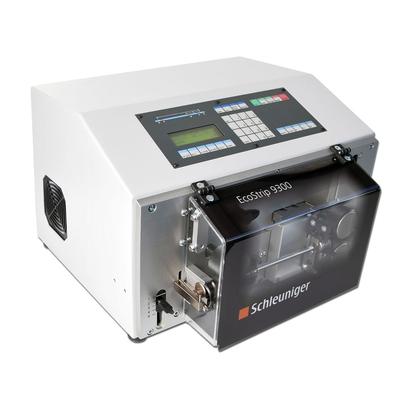
New Equipment | Cable & Wire Harness Equipment
Overview The all-electric EcoStrip 9300 efficiently and precisely processes round cables and wires up to 6 mm (0.235") outer diameter and flat ribbon cables up to a width of 13 mm (0.511") with a stripping length up to 999.9 mm (3.28 ft). Exce
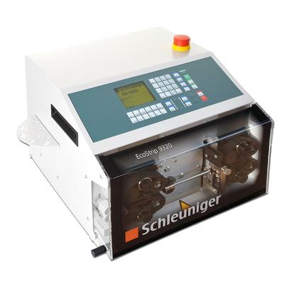
New Equipment | Cable & Wire Harness Equipment
Overview The powerful EcoStrip 9320 processes round cables up to 9 mm (0.35") O.D. and flat ribbon cables up to 13 mm (0.51") width with pull-off lengths up to 110 mm (4.33") on the right end (leading end) and 45 mm (1.77'') on the left end (traili
| 1 |


