
The Evolution 6 is designed to deliver zero defect soldering at high conveyor speeds with all flux types including conventional solvent based, water based, water soluble and VOC free; giving contract assemblers the freedom to change process technolog
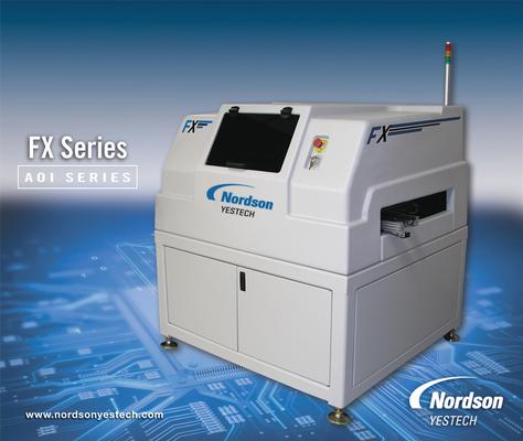
500,000 components per hour Maximum Board Size: 22” x 20” (560mm x 510mm) Clearance: 2” (50mm) top and bottom Minimum Component Size: 0201; 01005 with high magnification option
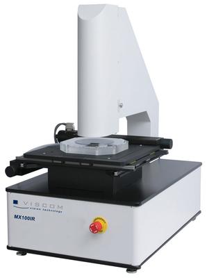
The Revolution is the easiest to use, most cost effective, high quality inspection system on the market. The Revolution is designed specifically for use on production lines and in failure analysis laboratories. Intuitive so
New ALPHA� Fluxes meet the challenges of both tin-lead and lead-free processes. ALPHA� EFSeries fluxes offer environmentally friendly benefits, while providing unmatched soldering performance. The ALPHA� flux line is unsurpassed in providing wave sol
At NBS, our manufacturing test engineers are highly experienced in the use of leading-edge automated inspection tools. We deploy proven automated X-ray inspection (AXI) and automated optical inspection (AOI) techniques to both identify manufacturing
New Equipment | Board Handling - Pallets,Carriers,Fixtures
* Provides dimensionally stable support platform for PCB * Protects SMT components from heat or thermal shock * Reduce/eliminate manual labor for hand masking operation, glue dotting, and hand soldering * Reduce solder defects (ex. Bridges and skips)
• Program Development and Delivery - Quality 5DX/x6000 automated X-ray inspection to uncover even marginal defects • Training - Basic and advanced training for programmers and repair operators • Component Testability - Determine the X-ray testab
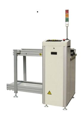
New Equipment | Board Handling - Conveyors
Connect with SMT and Al production lines. Safety design ensures not to break any PCB when it is pushed and thus reduce defect rate. Agility operation. With high accuracy, automatic counting, fault alarm functions, it is required for a full range of a
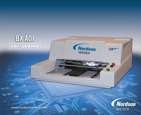
500,000 components per hour Maximum Board Size: 18” x 20” (457mm x 508mm) Clearance: 2” (50mm) top and bottom Minimum Component Size: 0201; 01005 with high magnification option
Automatic, High Accuracy Desktop Wafer Inspection For semiconductor assemblies, the requirement for a precise, thorough inspection for damage and defects during the production process is especially high. Wafers need non-destructive inspection of sur

.gif)


