New Equipment | Rework & Repair Equipment
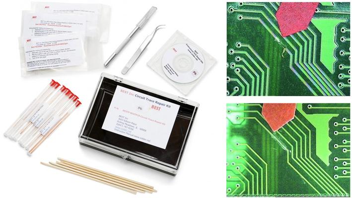
The BEST PCB circuit trace repair kit gives you the tools you need for fast modification and repair of PCB circuit traces. Our online PCB repair training videos, our master instructors along with these materials allows you to meet the original PCB qu
New Equipment | Rework & Repair Equipment
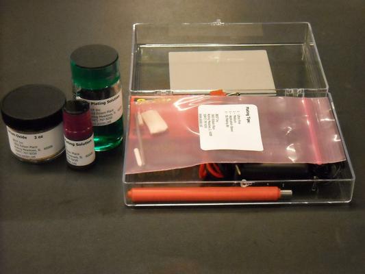
The BEST Gold Contact Replating Kit includes the tools you need for fast replating and modification of circuit contacts. Edge contacts may require replating if they are contaminated with solder or become scratched during handling or do not meet the m
New Equipment | Rework & Repair Equipment
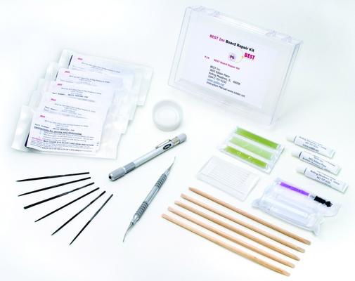
Poor handling procedures may sometimes damage corners and edges on printed circuit boards. Most of these types of damage to PCB's can be repaired using the BEST Board Repair Kit. This versatile repair kit along with our clear "how to" instructions of
New Equipment | Solder Paste Stencils
Eliminate hours of solder mask damage repair time for bga sites while improving rework yield. Are you frustrated by the time it takes to repair mask damage underneath the BGA during the rework process? Are you squeezed for space on the PCB in an
New Equipment | Fabrication Services
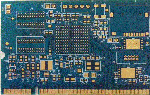
Minimum line width/space: 4mils Surface finish: immersion gold Board thickness: 1.20MM Minimum drilled hole diameter: 8mils Copper thickness: 0.5oz Special process : 0.40MM BGA , golden fingers
New Equipment | Fabrication Services
Our Service PCB Assembly and PCB&PCBA design are our main business.We are able to undertake a high quality Printed Circuit Board Assembly on competitive prices and flexible conditions.We are a complete “One- Stop” resource for printed circuit board
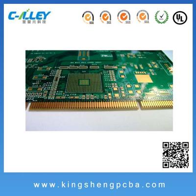
FR4 2. 0mm, red soldermask, Immersion gold+golden finger
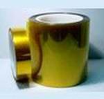
Features & Application: 1) Material: polyimide film 2) Imported organic silicone pressure - sensitive adhesive is introduced 3) High temperature resistant 4) Acid and alkaline resistant 5) Solvent resistant 6) Electrical insulation (Grade H) 7) Radia

New Equipment | Assembly Services
The board is designed by customer and it's for Air Purification control PCBA board. We did one-Stop EMS Service for this project (PCB manufacture, components sourcing, SMT and THT assembly): Product name: 2 Layer PCBA board Material: FR-4 Thicknss:
New Equipment | Assembly Services
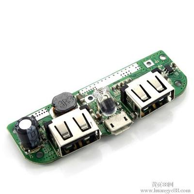
The board is designed by customer and it's for Power Bank PCBA board. We did one-Stop EMS Service for this project (PCB manufacture, components sourcing, SMT and THT assembly): Product name: 2 Layer PCBA board Material: FR-4 Thicknss: 1.6mm Surface:

Golden State is a contract manufacturer that makes wire harnesses, electromechanical assemblies (box builds, subassemblies, PCBAs, kits, etc.) and services (sorting, rework, value additive manufacturing engineering)
18220 Butterfield Blvd
Morgan Hill, CA USA
Phone: 5102268155


winsouce.jpg)