New Equipment | Test Equipment
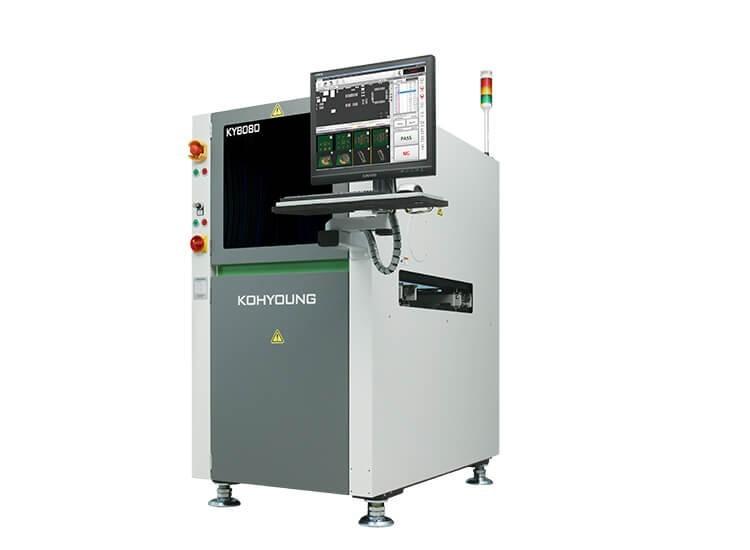
Koh Young KY8080 3D SPI Min component: 01005 PCB size:350x330mm Dimension:1000x1335x1627mm weight:600kg Product description: Koh Young KY8080 3D SPI, Min component: 01005, PCB size:350x330mm, weight:600kg, Dimension:1000x1335x1627mm Koh Young KY808
New Equipment | Test Equipment
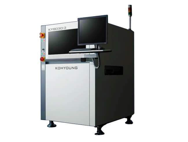
Koh Young KY8030-3 3D Inline SPI component Range: 01005 PCB size:350x330mm Dimension:1000x1335x1627mm weight:800kg Product description: Koh Young KY8030-3 3D Inline SPI, component Range: 01005, PCB size:350x330mm, Dimension:1000x1335x1627mm, weight:
500,000 components per hour Maximum Board Size: 22” x 20” (560mm x 510mm) Clearance: 2” (50mm) top and bottom Minimum Component Size: 0201; 01005 with high magnification option
500,000 components per hour Maximum Board Size: 18” x 20” (457mm x 508mm) Clearance: 2” (50mm) top and bottom Minimum Component Size: 0201; 01005 with high magnification option
1.5 million components per hour Maximum Board Size: 20” x 21” (500mm x 525mm) Clearance: 2” (50mm) top and bottom Minimum Component Size: 0201; 01005 with high magnification option
3550 sq. mm second (> 5.5 sq. in / second) Maximum Board Size: 350mm x 250mm (14 x 10 in.) Minimum Board Size: 50mm x 50mm (2 x 2 in.) Topside Clearance: 25mm (1 in.) Bot
3550 sq. mm second (> 5.5 sq. in / second) Maximum Board Size: 350mm x 250mm (14 x 10 in.) Minimum Board Size: 50mm x 50mm (2 x 2 in.) Topside Clearance: 25mm (1 in.) Bot
Solder joint inspection of bottom-side PCBs Intelligent Inspection of Solder Joints, THT and SMD Components Today, the industry standard quality assurance in electronics production is automatic optical inspection (AOI) of SMD components on printed
SUPERIOR VISION 4000 � SUPERIOR SOLDER DEFECT DETECTION The Photon Dynamics Superior Vision (SV) 4000 AOI system delivers comprehensive defect detection. Designed for high-pulse production of large-format, high-density and small component PWAs, t
SUPERIOR VISION 6000 � UNRIVALED SOLDER DEFECT DETECTION The Photon Dynamics Superior Vision (SV) 6000 AOI system delivers comprehensive defect detection. Designed for high-pulse production of large-format, high-density and small component PWAs,


