New Equipment | Test Equipment
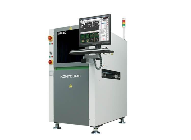
Koh Young KY8080 3D SPI Min component: 01005 PCB size:350x330mm Dimension:1000x1335x1627mm weight:600kg Product description: Koh Young KY8080 3D SPI, Min component: 01005, PCB size:350x330mm, weight:600kg, Dimension:1000x1335x1627mm Koh Young KY808
New Equipment | Test Equipment
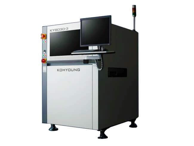
Koh Young KY8030-3 3D Inline SPI component Range: 01005 PCB size:350x330mm Dimension:1000x1335x1627mm weight:800kg Product description: Koh Young KY8030-3 3D Inline SPI, component Range: 01005, PCB size:350x330mm, Dimension:1000x1335x1627mm, weight:
500,000 components per hour Maximum Board Size: 22” x 20” (560mm x 510mm) Clearance: 2” (50mm) top and bottom Minimum Component Size: 0201; 01005 with high magnification option
500,000 components per hour Maximum Board Size: 18” x 20” (457mm x 508mm) Clearance: 2” (50mm) top and bottom Minimum Component Size: 0201; 01005 with high magnification option
1.5 million components per hour Maximum Board Size: 20” x 21” (500mm x 525mm) Clearance: 2” (50mm) top and bottom Minimum Component Size: 0201; 01005 with high magnification option
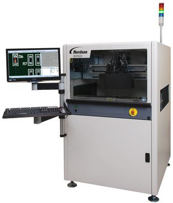
3550 sq. mm second (> 5.5 sq. in / second) Maximum Board Size: 350mm x 250mm (14 x 10 in.) Minimum Board Size: 50mm x 50mm (2 x 2 in.) Topside Clearance: 25mm (1 in.) Bot
3550 sq. mm second (> 5.5 sq. in / second) Maximum Board Size: 350mm x 250mm (14 x 10 in.) Minimum Board Size: 50mm x 50mm (2 x 2 in.) Topside Clearance: 25mm (1 in.) Bot
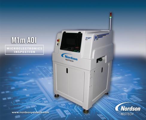
SUPERIOR VISION 4000 � SUPERIOR SOLDER DEFECT DETECTION The Photon Dynamics Superior Vision (SV) 4000 AOI system delivers comprehensive defect detection. Designed for high-pulse production of large-format, high-density and small component PWAs, t
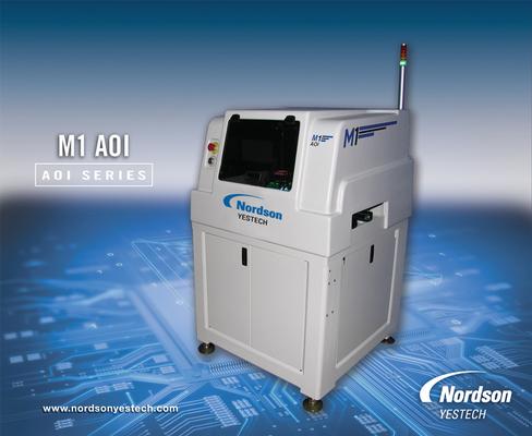
SUPERIOR VISION 6000 � UNRIVALED SOLDER DEFECT DETECTION The Photon Dynamics Superior Vision (SV) 6000 AOI system delivers comprehensive defect detection. Designed for high-pulse production of large-format, high-density and small component PWAs,

New Equipment | Solder Paste Stencils
DEK’s Nano-ProTek technology is a permanent, hydrophobic nano-coating that, when applied to the bottom-side of the stencil foil and stencil aperture walls, minimizes solder paste’s ability to stick to the foil surface. Up to a 10X increase in the num


