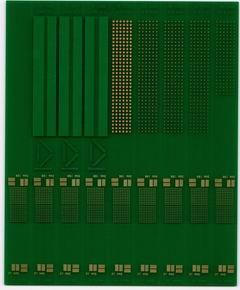
Capabilities include: 1 to 20 layers, adhesive based or adhesiveless, 3 mil traces and spaces, 6 mil drilled holes, available in 3 days to 20 days
Capabilities include: 2 to 20 layers, 3 mil traces and spaces, 6 mil bond pitch, 6 mil drilled holes, internal cavity and consistent wire bondable gold.
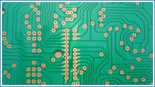
min trace width/space 3 mils, min hole diameter 0.15mm

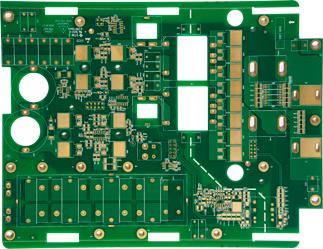
Layer: 12 Material: FR4(Tg170) Board thickness: 1.6mm Min trace width/spacing: 4/4mil Min hole size: 0.2mm Impedance control

Are you looking for a professional and easy-to-use PCB Design software with powerful autorouter and reasonable price? Try DipTrace and you will be surprised! DipTrace is a complete state-of-the-art PCB Design System. It includes: PCB Layout — PCB
Up to 30 layers, down to 3 mil traces / spaces, 6 mil drilled holes. MIL-P-55110 approved for FR-4, polyimide, PTFE, epoxy Thermount(tm). Copper Sealed Vias are available. Deliveries down to 24 hours are available.
eavy copper board Material FR-4 Layers : 2 Trace width/space : 10 mil/10 mil Copper thickness 5/5 oz Application : High Voltage power Supply
Heavy copper PCB/ Power supply PCB Layer: 4 Material: FR4(Tg170) Finished copper thiness:4oz on each layer Min. trace width/spacing: 0.3/0.4mm(12/16mil) Application: Power controls, heat dissipation

In accordance with Spec information such as layer count, trace width, trace spacing, drill size and business information such as due date, shipping method, place of delivery, the system will search the manufacturers who are most suitable to produce t
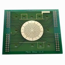
General specification for Microwave/RF PCB Layer count: 1-6 Board thickness: 0.2-3.2mm Copper thickness: 0.5-4oz Dielectric Constant(DK): 2.2-10.3 Min trace width/spacing: 4/4mil Min drill hole size: 0.2mm Surface treatment: HAL(Lead free), I


