
New Equipment | Fabrication Services
Printed Circuit Boards: Our association includes several manufacturing houses UL, ISO, Mil-P-55110, and Mil-P-31032 approved and certified which between them have the following capabilities: � 1-30 layers � Minimum line width and space of .003 & .0
Mix high frequency material (basic stack up): | --- ---------- LAYER 1 (TOP LAYER) 0.5OZ+PLATE | Pre-Preg 10MIL RO4350B | ---------- LAYER 2 (MID LAYER 1) 0.5OZ 1.6 mm +/-10% Core FR-4

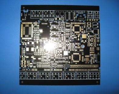
Layer: 2 Material: FR-4 Board Thickness: 1.6mm Surface Finish: HAL Copper Thickness: 2/2 oz Green Solder Mask Layers: 2--36layers Max manufacturing size: 640mm*1100mm Copper foil thickness: 0.5OZ-13OZ Min line width/space: 3mil/3mil Min
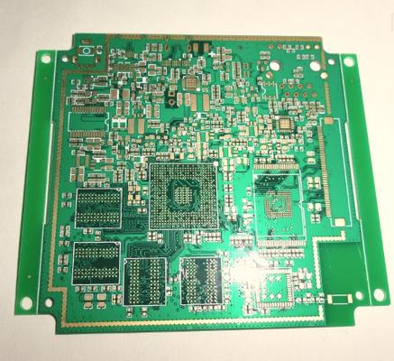
Layer: 6 layers Material: FR-4 Board Thickness: 1.0mm Surface Finish:ENIG Copper Thickness: 1 oz all layers Blind via L1~L2 and L1~L3 Layers: 2--36layers Max manufacturing size: 640mm*1100mm Copper foil thickness: 0.5OZ-13OZ Min line width
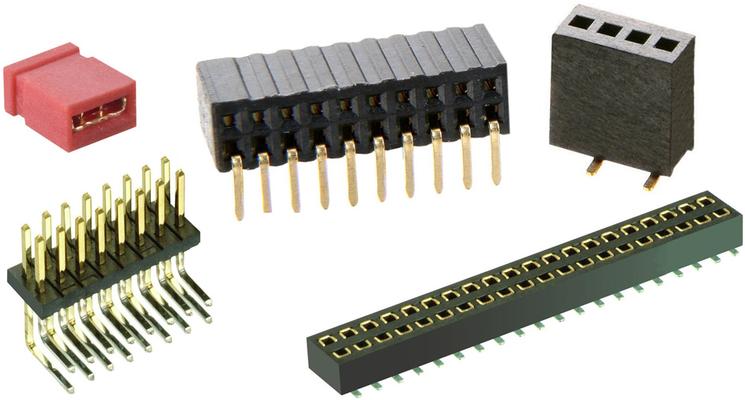
Our range includes board to board and cable to board connectors in a variety of high-reliability, high performance interconnect styles, and industry standard interconnect. Harwin connectors are available from our global distribution network. Harwin
New Equipment | Cable & Wire Harness Equipment
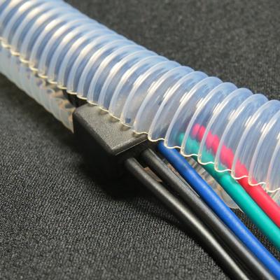
Convoluted PTFE Tubing ( SAE-AS81914/1 or M81914/1 ) is engineered to be an equivalent to that of Corrugated FEP Tubing where sharp turns and small band diameters are needed. It can be used as an electrical or fluid conduit in the semi conductor indu
RollPruf tri-polymer blend of neoprene, nitrile and natural rubber in 8 mil, hand specific design provides optimum comfort, reduced hand fatigue, with durability and strength uncommon to latex gloves. Applications: Chip Assembly Photomask Assembly Ph
NiProtect gloves are 4 mil, 100% nitrile ambidextrous design to provide superior tactility, puncture and abrasion resistance and available in 10" or 12" lengths. Applications: EMS Laboratory/Research Patient Examination Precision Parts Handling Proce
.Hardware development: Analog- und digitaltechnique, highfrequenztechnique Intel, Motorola, SPS, TI DSP AT-, SCSI-, VME-, MIL-, CAN-Bus .Software development: DOS, Windows 3.1x/95/NT, UNIX Assembler, Basic, ADA, FORTRAN, Pascal, Delphi, C/C++ (Borlan
Ridgid, bare board manufacturing of military, high reliability, quick-turn, prototype, single, double-sided, and multilayer boards, blind and buried vias, carbon ink, immersion silver, immersion tin, reflow, hasl, nickel and gold, all colors of legen


