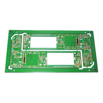
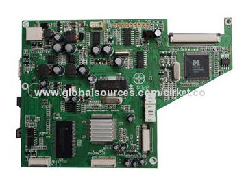
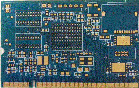
Materials: FR-4 Copper Thickness: 3 oz Layer Count: 6 Layer, 1.6 mm Min. Hole Size: 12 mil Min.Line Width/Space: 6 mil Finishing : Immersion Gold
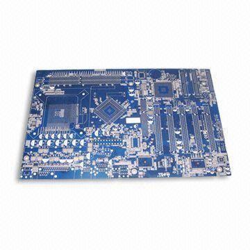
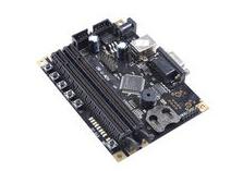
Materials: FR-4 Copper Thickness: 1 oz Layer Count: 4Layer, 1.6 mm Min. Hole Size: 12 mil Min.Line Width/Space: 8 mil Finishing: Immersion Gold + Carbon ink
New Equipment | Assembly Services
1,012 (normal) Electric strength: >1.3kV/mm Thermal stress: 288°C, 20 seconds Test voltage: 50 to 300V
New Equipment | Assembly Services
1,012 (normal) Electric strength: >1.3kV/mm Thermal stress: 288°C, 20 seconds Testing voltage: 50 to 300V Packing: vacuum packing for PCB, and good condition outer boxes
New Equipment | Fabrication Services
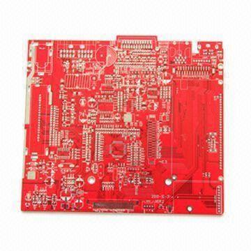
ENIG PCBs with red soldermask Layers: 2 Base material: FR4 Copper thickness: 1oz Board thickness: 1.6mm Min. hole size: 0.45mm Min. line width: 3 mils Min. line spacing: 3 mils Surface finishing: HASL
New Equipment | Fabrication Services
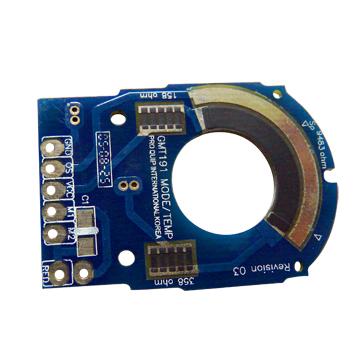
Layers: 2 Base material: FR4 Copper thickness: 1oz Board thickness: 1.6mm Min. hole size: 0.45mm

New Equipment | Fabrication Services
Layers: 2 Base material: FR4 Copper thickness: 1oz Board thickness: 1.6mm Min. hole size: 0.45mm
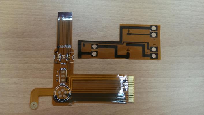
1~6 layers, based film PI and PET, RA/ED Copper, Coverlay 0.50~2.0mil, Min. line/space +/-2mil, Outline by routing and laser cut. Sample lead time 5~7 days, mass production 10~14 days.
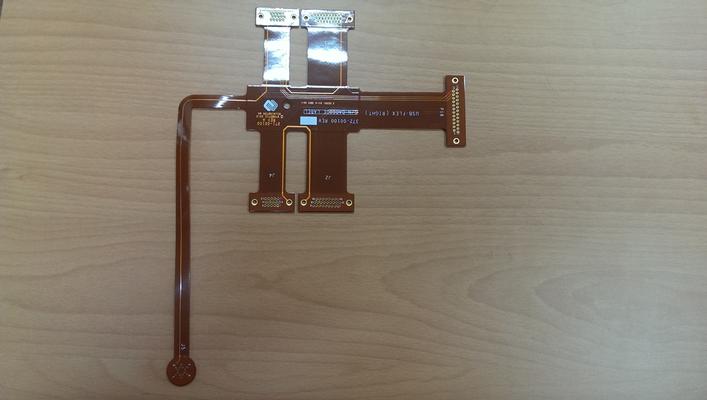
1~6 layers, based film PI and PET, RA/ED Copper, Coverlay 0.50~2.0mil, Min. line/space +/-2mil, Outline by routing and laser cut. Sample lead time 5~7 days, mass production 10~14 days.
New Equipment | Fabrication Services
Minimum line width/space: 4mils Surface finish: immersion gold Board thickness: 1.20MM Minimum drilled hole diameter: 8mils Copper thickness: 0.5oz Special process : 0.40MM BGA , golden fingers


.png)


