New Equipment | Solder Materials
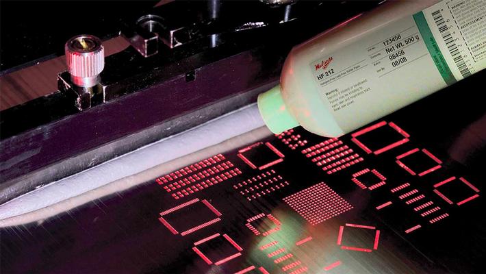
8 hours), and abandon time (>4 hours) Printing: Suitable for high speed printing up to 150 mm/s Reflow: Solderable on challenging surface finishes (CuNiZn and Copper OSP) Colorless residues for easy post-reflow inspection Careful contr
Oak-Mitsui is recognized as the technological leader in the manufacture of high-quality electrodeposited copper foils for the printed circuit board industry. With the strength of international scope, Oak-Mitsui produces both conventional cladding and

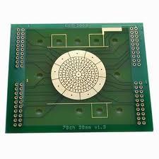
1) Single Sided PCB 2) Material ranges: FR-1, 94VO/HB, 22nf, CEM-1 and CEM-3, FR-4 3) Copper weight: 1-2 oz 4) Profile: Punch 5) Thickness: 0.8mm-1.6mm 6) Surface finish: OSP, HASL, Immersion Gold
Pan-Continental (H. K.) Limited. Fax: 886-4-26811523 Tel: 886-4-26819543 Email: pcc01@zinc.com.tw Dir Sir, 04Mar2002 Re: Copper Oxide We can offer CuO as the following spec., which suitable for electronic area expecial PCB industr
New Equipment | Solder Materials
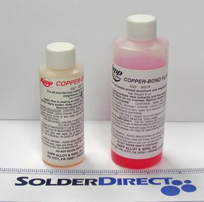
Flux designed specifically to work with KappZapp7, 7.0% Silver solder to remove the oxide layer on Copper to allow a strong metallic bond between the solder and the base metal. Its active range is 500°F - 750°F (260°C - 390°C). Kapp Copper-Bond Flux
New Equipment | Solder Materials
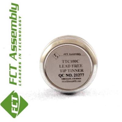
Tip tinner to aid in cleaning and re-tinning solder iron tips de-wetted by use which can’t be repaired with sponge pads and cored solder wire. Use of TTC100C LEAD FREE Tip Tinner offers the following advantages: Lead Free SN100C tin/copper/nic
General specification for Microwave/RF PCB Layer count: 1-6 Board thickness: 0.2-3.2mm Copper thickness: 0.5-4oz Dielectric Constant(DK): 2.2-10.3 Min trace width/spacing: 4/4mil Min drill hole size: 0.2mm Surface treatment: HAL(Lead free), I
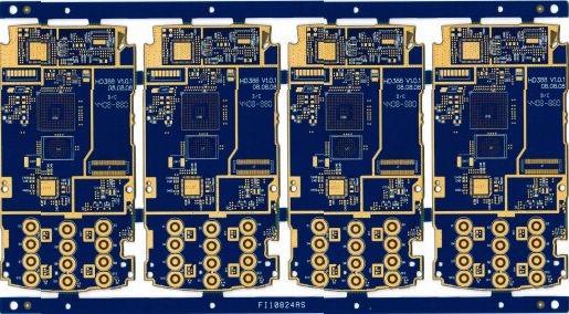
High-density interconnection/HDI PCB Layer: 8 (HDI) Structure: 2+4+2 with stack via Material: FR4(Tg170) Thiness: 1.0mm Surface treatment: Selective immersion gold + OSP Blind via L1-2 & L2-3 & L6-7 & L7-8: 0.1MM (4mil) Buried via L3-6:
Layer: 8 layers Material: FR-4 Board Thickness: 0.6mm Surface Finish: Immersion Gold 1~4u Copper Thickness: 1/3 oz Impedance, 4/4mils width/spacing Layers: 2--36layers Max manufacturing size: 640mm*1100mm Copper foil thickness: 0.5OZ-13OZ M

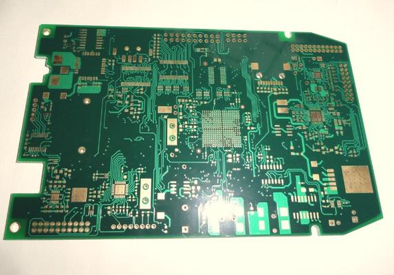
Layer: 2 Material: FR-4 Board Thickness: 1.6mm Surface Finish: HAL Copper Thickness: 2/2 oz Green Solder Mask Layers: 2--36layers Max manufacturing size: 640mm*1100mm Copper foil thickness: 0.5OZ-13OZ Min line width/space: 3mil/3mil Min


