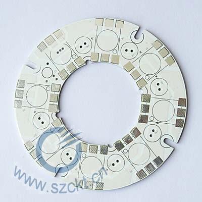
Aluminium PCB Materials: Aluminium.This material is made in China and has big competitive price. Layer Number: 1 Board thickness: 1.0mm Surface technique: Pb free HAL Minimum hole size: 0.30mm Minimum Line/Space: 0.25mm/0.25mm Solder mask: Blac

Layer: 2 Material: FR-4 Board Thickness: 1.6mm Surface Finish: HAL Copper Thickness: 2/2 oz Green Solder Mask Layers: 2--36layers Max manufacturing size: 640mm*1100mm Copper foil thickness: 0.5OZ-13OZ Min line width/space: 3mil/3mil Min
New Equipment | Assembly Services
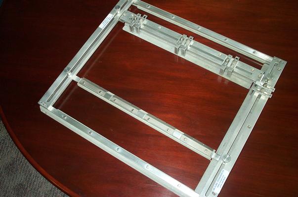
WORK BOARD HOLDERS TOOLING TO HOLD PRINTED CIRCUIT BOARD IN PLACE OVER INSERTION & PICK AND PLACE MACHINE SELECTIVE SOLDER PALLETS TO ELIMINATE MANUAL MASKING OF PRINTED CIRCUIT BOARD'S BEFOR THEY GO OVER WAVE. PALLETS HELP WITH DEFECTS AND E
New Equipment | Rework & Repair Equipment
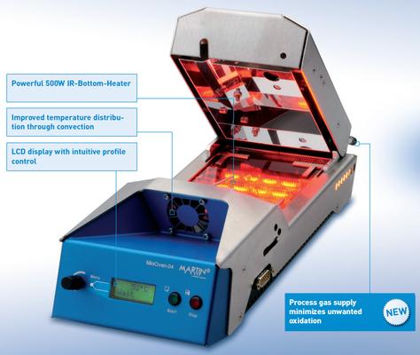
Desktop Reflow Oven For Reballing and Prebumping of SMD Components The new MiniOven-04 is perfectly suitable for a wide range of applications, from small QFNs to very large BGAs. This is due to our extensive selection of stencils and masks for almos
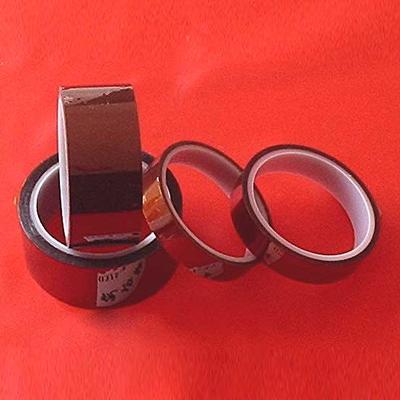
Polyimide tape can either be amber or clear in color, and the film thickness ranges 1 and 3 mils while the adhesive may range from 1 to 2 mils thick. It may be double sided, and the adhesive may be silicone or acrylic based. Anti-static Polyimide t
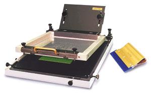
Cost effective manual stencil printer designed for low to medium volume assembly production runs. The SPR-20 benchtop, manual stencil printer is designed for low to medium volume assembly runs. Precise X,Y, Z, and theta axis controls allow for accur
Printed Circuit Board Prototypes. PNC Specializes in Quick Turn Prototype PCBs starting at 24 Hour turn times without sacrificing Quality. We have been the Leader of quick turn for 45 Years using the latest Manufacturing processes and equipment. Ou
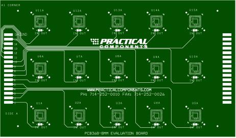
PC boards and kits for machine set-up and calibration, hand solder training, rework, practice, testing and more along with a drawing of each PCB. Practical has a PCB board or kit to meet your requirements. BGA Fine Pitch, Global Daisy-Chain or Vari
New Equipment | Assembly Services
PCB process capability Base material: CM1, CM3, FR1, FR4, Metal based Layer: 1 to 24 layers Board thickness: 0.4mm to 3mm Copper thickness: 0.5oZ, 1oZ, 2oZ Min Copper thickness in hole: 0.02mm Max working size: 400*610mm Surface finishing: HAS
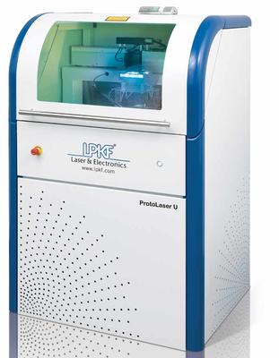
The next generation of in-house prototyping Laser-based PCB production can achieve much greater circuit detail, and lasers structure circuits significantly faster. This technology provides true on-demand production solution for both prototyping and


