New Equipment | Solder Paste Stencils
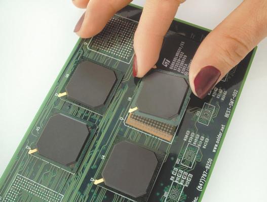
Eliminate hours of solder mask damage repair time for bga sites while improving rework yield. Are you frustrated by the time it takes to repair mask damage underneath the BGA during the rework process? Are you squeezed for space on the PCB in an
Lite Fast SR-1000, a UV Solder Mask, was designed to screen print over conductive traces, landing pads, resistors, fuses and capacitors on Printed Circuit Boards (PCBs) and ceramic substrates. Other applications include metal and various plastics.
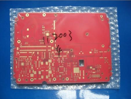
1). Size: 45*140mm/1 up 2). Layer count: 2 Layer, 20 μm PTH 3). Thickness: 1.6mm +/- 10% 4). Copper weight(Finished): 35 μm 5). SMOBC: LPI Green solder mask/ White legend 6). Holes: 0.4mm minimum, 4/4 mil track/space 7). Pads finish: HASL 8).
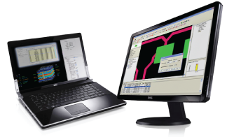
Design For Manufacturability And Yield Enhancement. The Design for Manufacturability (DFM) engine searches for fabrication issues and discovers areas where yields may be increased. GraphiCode's Contour Technology produces fast and accurate results f
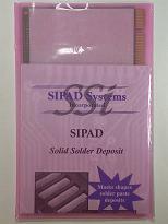
SIPAD Solid Solder Deposit (ssd) is a Siemens patented process that pre loads the pc board surface mount pads with solder in a solid form. Boards are printed, reflowed without components producing a predictable repeatable meniscus. SIPAD boards a

The most reliable 3D data and 100 % inspection Our innovative 3D laser triangulation sensor, the RSC profiles real shape of features and also provides highly robust 3D data against considerable variations of PCB color and finishing condition, solde

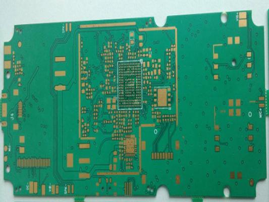
Layer: 2 Material: FR-4 Board Thickness: 1.6mm Surface Finish: HAL Copper Thickness: 2/2 oz Green Solder Mask Layers: 2--36layers Max manufacturing size: 640mm*1100mm Copper foil thickness: 0.5OZ-13OZ Min line width/space: 3mil/3mil Min
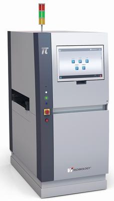
PI Series is a new generation 3D Solder Paste Inspection system that overcomes the limitations of traditional SPIs and satisfy all your inspection needs. The PI Series allows to easily implement Solder Paste Inspection in any PCBA line. These new ge
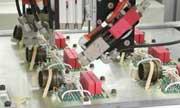
New Equipment | Assembly Services
Quick turn Prototype PCBs from 24 hour turnaround to high volume printed circuit board production from our domestic plant in USA and/or China facilities. Our Modern 38,000 sq. ft. manufacturing plant with multi-million dollar investment with latest e
New Equipment | Fabrication Services
8 Layers Printed Circuit Boards Manufacturing Multilayer PCB Fabrication Product Name: Multilayer PCB Board Material: FR4 Copper thickness 1 oz all layers Board Thickness: 1.6mm Special requirement Impendence Control Fab by Circuit Boar


.png)

