
eFlex Track & Trace is a manufacturing traceability and quality control software solution which enables users to store, retrieve, and report part status in a manufacturing environment. Using state-of-the-art server software, in conjunction with strea
40mm Applications Solder Joint Quality (BGA, Leaded) Bridging Voiding Opens Bare boards (Inner layers, traces, vias) Component Package Inspection (wire bonds) Subtle Defect Inspection
New Equipment | Assembly Services
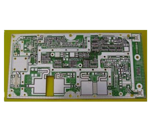
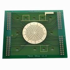
4 layer PCB Material: Rogers 5880 Finished Thickness :2.0 mm; Copper thickness : 1OZ finished ; Surface finishing: Immersion Tin Min Via hole size :0.30mm; Min Trace width/ spacing : 0.13 mm / 0.13 mm
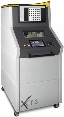
New Equipment | Test Equipment
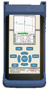
850/1300/1310/1550nm Quad Viper OTDR The TTI FTE-7000 OTDR is fast, easy to use, affordable and rugged. It has a short dead zone, bright 4 inch color display and with an onboard context sensitive help system the OTDR has a minimal learning curve fo
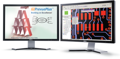
In response to many inquiries from GC-Prevue users, GraphiCode created GC-PrevuePlus to fill the need for an inexpensive Gerber translator and editor. Building on proven functionality from GraphiCode's existing family of products, GC-PrevuePlus takes
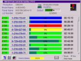
TIMMS PCS (Parts Control System): Demand Chain Management � full material control and trace-ability featuring electronic 'kanban' system, direct pull-signal from the process, reduced WIP, elimination of feeder placement errors. Direct communication w
New Equipment | Test Equipment
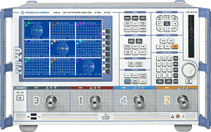
50 dB High speed o Measurement time o Switching time between channels o Switching time between instrument setups o Data transfer time o Simultaneous measurement of more than one DUT Modern user interface o Intuitive Windows-based
New Equipment | Test Equipment
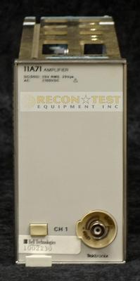
The single-channel 11A71 is the highest bandwidth amplifier currently available for the Tektronix 11000-series mainframes. It provides 1 GHz bandwidth in the 11402 digitizing mainframe and 500 MHz bandwidth in the 11401 digitizing mainframe and 11302
General specification for Microwave/RF PCB Layer count: 1-6 Board thickness: 0.2-3.2mm Copper thickness: 0.5-4oz Dielectric Constant(DK): 2.2-10.3 Min trace width/spacing: 4/4mil Min drill hole size: 0.2mm Surface treatment: HAL(Lead free), I
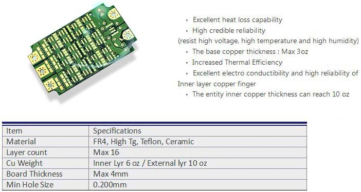
Heavy copper can be used in a PCB for a variety of purposes, including high power distribution, heat dissipation, planar transformers, and power convertors. Mapletech has been building heavy copper circuit boards with traces and copper planes of up


