New Equipment | Assembly Services
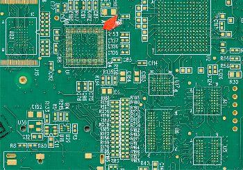
10-Layer Via-in-Pad Technology PCB features blind via in L9-10 in addition to the Fine Pitch BGA. Putting the via in the pad creates space on the external layers for more routing and avoids potential shorts during assembly. The routing channel widt
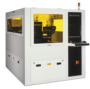
The 3D Profiler is an automatic machine to measure the dent of the copper filled vias. The system offers the opportunity for 100% inspection to ensure the yield of the copper filling with inspection speeds of 5 minutes per panel and +/- 2 micron accu
Fab technology includes; 3 mil trace, 5 mil vias, micro SMT & BGA, controlled impedance, high speed dielectric laminates, blind & buried vias.
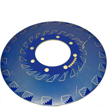
This 26-layer Stator board features 7 ounce layers (182oz total), and ENIG finish and Blind and Buried Vias.
High-density interconnection/HDI PCB Layer: 8 (HDI) Structure: 2+4+2 with stack via Material: FR4(Tg170) Thiness: 1.0mm Surface treatment: Selective immersion gold + OSP Blind via L1-2 & L2-3 & L6-7 & L7-8: 0.1MM (4mil) Buried via L3-6:
Double Sided and Multilayer Interconnects. PTH, SMT, BGA, and laser via technologies.
MIL-P-55110 approved for PTFE materials. Capabilities include PTFE, Thermoset materials, PTFE/FR4 hybrids, edge plating, wrap-around fingers and copper sealed vias.
Using all PTFE, Thermoset and other high performance materials, including epoxy / PTFE hybrids, edge plating and copper sealed vias.
DVD authoring VCD authoring SVCD authoring Virtual Reality authoring Vrtual Visualization of Industrial Prototypes and e-Commerse marketing via Internet
Multilayer PWBs BGA MCM Blind/Buried Via Buried Capacitance Buried Resistance Impedance Controlled


