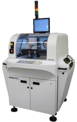
Precision Dispensing System for Heated Dispense Applications The GPD Global MAX II is a compact; high-accuracy system designed for today’s advanced heated dispensing applications. The frame is molded from “liquid rock” which gives the system a stabl
If you have only Gerber data files to work with then ProntoGERBER-CONNECTION can help you! ProntoGERBER-CONNECTION imports raw Gerber data and allows the user to add intelligent information to the shapes on the display and create process assembly
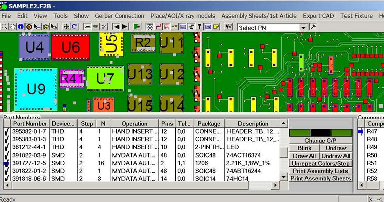
ProntoVIEW-MARKUP is assembly CAD Viewer & Gerber Viewer software used by electronics manufacturers to quickly find components, pin, shorts between traces, etc. ProntoVIEW-MARKUP is also a redline tool that allows annotation of the assembly to creat
New Equipment | Solder Paste Stencils
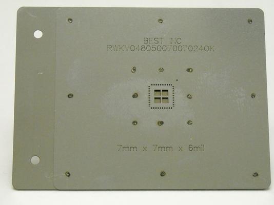
Based on its long work on BGA rework and repair process and its in-house capability to produce metal stencils BEST can provide for you a timely, cost-effective solution for printing on to components for MOST rework systems. Our templates for printin
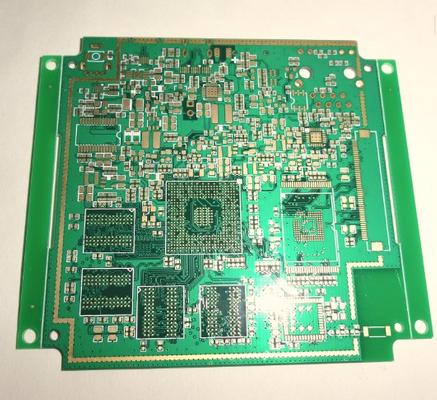
Layer: 6 layers Material: FR-4 Board Thickness: 1.0mm Surface Finish:ENIG Copper Thickness: 1 oz all layers Blind via L1~L2 and L1~L3 Layers: 2--36layers Max manufacturing size: 640mm*1100mm Copper foil thickness: 0.5OZ-13OZ Min line width
New Equipment | Design Services
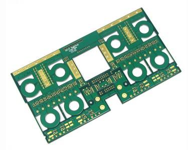
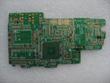
Layer:4 Material:FR-4 4/4/4/4oz Thickness:2.0 Minimum hole:0.35mm Minimum Tracc/Spacing:12mil/15mil Application:power supply Layers: 2--36layers Max manufacturing size: 640mm*1100mm Copper foil thickness: 0.5OZ-13OZ Min line width/space:
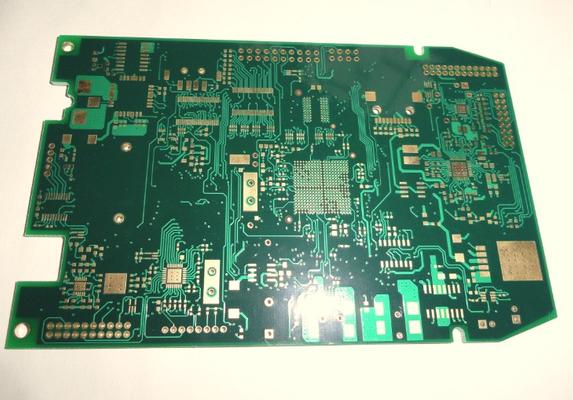
Layer: 8 layers Material: FR-4 Board Thickness: 0.6mm Surface Finish: Immersion Gold 1~4u Copper Thickness: 1/3 oz Impedance, 4/4mils width/spacing Layers: 2--36layers Max manufacturing size: 640mm*1100mm Copper foil thickness: 0.5OZ-13OZ M

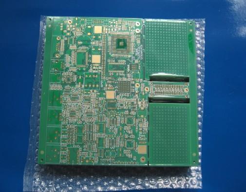
Layer: 2 Material: FR-4 Board Thickness: 1.6mm Surface Finish: HAL Copper Thickness: 2/2 oz Green Solder Mask Layers: 2--36layers Max manufacturing size: 640mm*1100mm Copper foil thickness: 0.5OZ-13OZ Min line width/space: 3mil/3mil Min
Bicheng provides impedance controlled PCB's for R&D, high-tech, IT research companies and organizations, large or small. Technical parameters *Controlled dielectric *Controlled impedance *Design coupons *Test coupons *Po
1. FR-4 Tg170 2. 20 layer, 1.6mm thick 3. 1 oz copper finished 4. 10% impedance control 5. Blind/buried vias 6. 0.1mm holes, HDI 7. Application: telecommunication, industrial control, medical equipment


