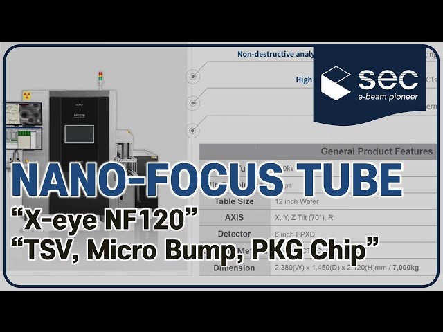
#Xray#Inspection#SEC Nano-focus Tube of 200 nano resolution which is specialized for sub-micron defects of Semiconductor Packaging, Wafer Level Packaging(WLP). -Non-destructive Analysis System -High-Resolution Image with Dual Type CTs -Application

Welcome to this Defect of the Month video on via hole failures and how to see them, this series of videos were produced for and featured as part of the NPL/IPC video library and examples are taken from the NPL Defect Database. Over the last couple of
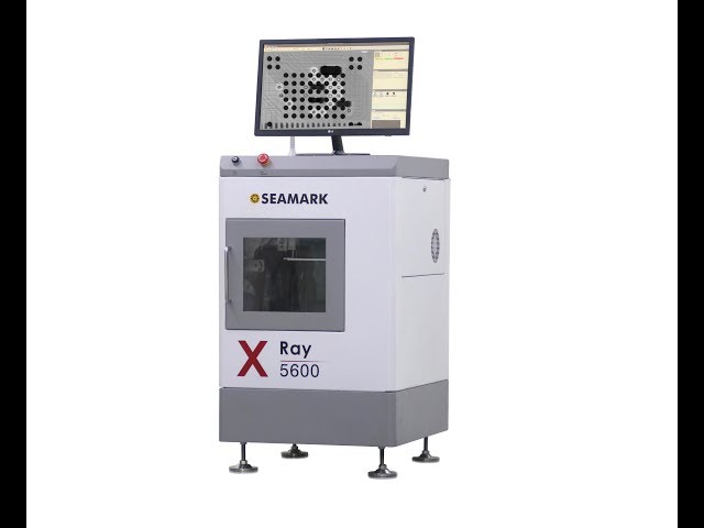
Shenzhen zhuomao is located in Shenzhen, China.SHENZHEN ZHUOMAO TECHNOLOGY CO.,LTD - Seamark Group The leading manufacturer of BGA/SMT rework, X-ray inspection system, TV LCD panel laser repair for 13 years in China. Established in 2005, we have coo

In this video we briefly demonstrate the removal of a BGA component from a smart phone circuit board. To get a quote or obtain more information on the IR 1000, visit the link below: https://www.paceworldwide.com/products/area-array-bga-rework/bga-r

http://yincae.com/index.html YINCAE SMT 256 Dipping Process YINCAE SMT 266 Jetting Process
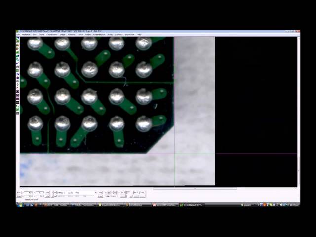
ScanCOMPONENT is a PC-based offline component programming system for the creation of vision data files from the smallest flip chip and bumped packages to the largest odd form devices. The ScanCOMPONENT is a standalone Product as well as a module of
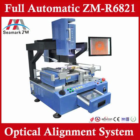
1.The top heater can move freely along the X, Y axis in the IR preheating area It is good for many BGA chips distribution at different positions in the PCB board which need repair X-shaped infrared laser can do rapid location After location the elect

Discover the RH-2000 from Hirox! More information: - www.hirox-europe.com - www.hirox.com - www.hirox-usa.com