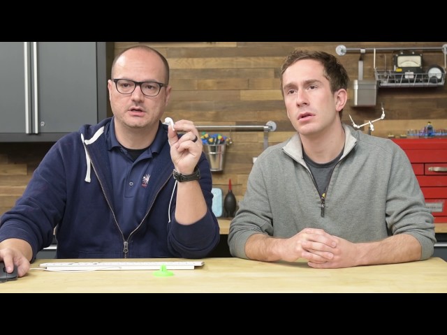
We stopped by ifixit for a chat about our new TruView Fusion CT - our 3D X-Ray system. And of course, we did a virtual teardown of the Apple AirPod, because we just can't help ourselves...
Stinger90 is an off-line X-ray inspection and industrial CT system with the highest voltage of 90kV, which is designed for electronic industry. It can meet the needs of X-ray inspection of PCB, SMT, small electronic components, semiconductor packagin

#xray#3DCT#SEC "SF160Series" ????? X-ray ?? ?? (F) ???, ?? ??? ?? ??? ?? 2D/3D CT ?? ?? (N) Hybrid Tube ??? 160F?? ????? ??? ?? ?? ?? Specifications X-ray Tube: 160kV / (F)200µA (N)500µA Min. Resolution : (F)0.9µm (N)0.8µm Table Size: 450X530 mm
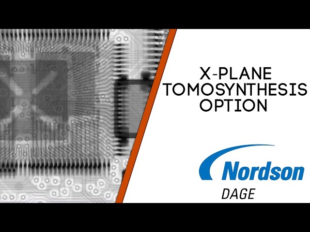
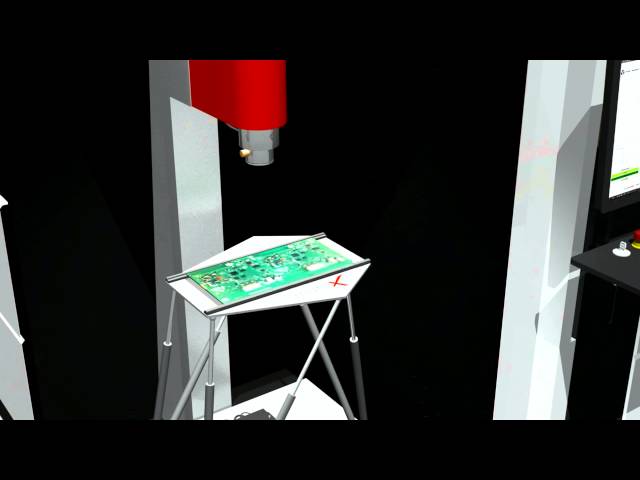
The X-Plane™ option uses a proprietary, patent applied for, tomosynthesis (or CT) technique to create 2-D X-ray slices in any plane of a printed circuit board assembly without the need to cut or destroy the board. In this way, the superior image qual
Manual and semi-automatic ?CT inspection systems for small electronic components with measurements of voxel sizes around 15 -- 20 ?m. Depending on customer requirements the system can equipped with the most suitable x-ray tube and detector.
The X-Plane™ option uses a proprietary, patent applied for, tomosynthesis (or CT) technique to create 2-D X-ray slices in any plane of a printed circuit board assembly without the need to cut or destroy the board. In this way, the superior image qual
Highly flexible, multi-axis inspection system featuring a parallel-kinematic Hexaglide manipulation unit that allows extreme off-axis X-ray transmission in the smallest of space with maximum speed and in high resolution. This technology is especially
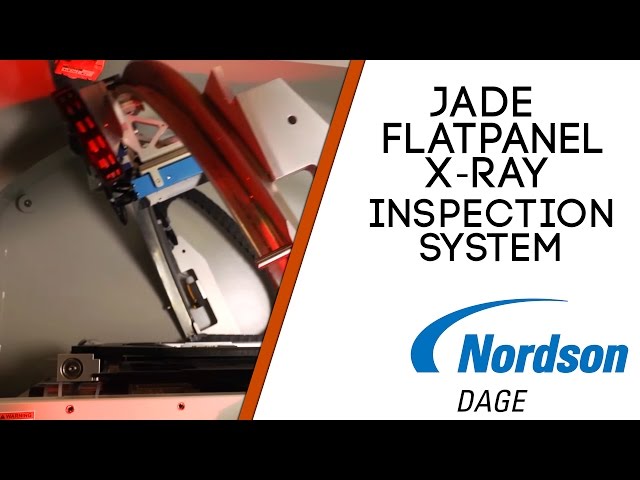
The new Jade FP is launched into an aggressive market sector where both value and performance must be met, an area in which Nordson DAGE already has a market-leading reputation. "Performance Beyond Expectations" is this exciting new system's slogan
The X-Plane™ option uses a proprietary, patent applied for, tomosynthesis (or CT) technique to create 2-D X-ray slices in any plane of a printed circuit board assembly without the need to cut or destroy the board. In this way, the superior image qual
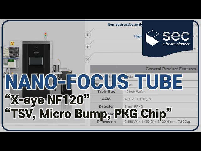
#Xray#Inspection#SEC Nano-focus Tube of 200 nano resolution which is specialized for sub-micron defects of Semiconductor Packaging, Wafer Level Packaging(WLP). -Non-destructive Analysis System -High-Resolution Image with Dual Type CTs -Application


.png)

