
Industry Directory | Other / Consultant / Service Provider / Media / Publisher / Online Resource
PCB Libraries' "Footprint Expert" suite uses CAD LEAP(tm) Technology to greatly simplify footprint and 3D STEP model creation; it is used by tens of thousands of PCB designers and engineers all over the world.
New Equipment | Rework & Repair Equipment
BEST HotDots™ are designed to simply and cleanly attach jumper wires on a board. HotDots™ are built to survive at high temperature as both the adhesive and the polyimide material are designed to withstand wash and reflow temperatures. HotDots™ are a
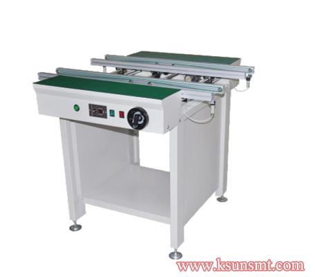
New Equipment | Board Handling - Conveyors
Model No: KSUN 250H Dual Track Conveyor Power supply: 100-230V AC (customized), single phase Power load: MAX 100V/A Transport direction: Left to right/right to left(optional) Transport height: 900±20mm (or customized) PCB thickness: Min 0.6mm
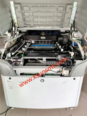
Used SMT Equipment | Screen Printers
DEK Horizon 03i automatic stencil printer Specification : DEK Horizon 03i High Precision Automatic Solder Paste Printer designed for high precision steel mesh printing or stencil printing in SMT industry. Printing PCB size: 50x50mm to 508x510mm;

Used SMT Equipment | Chipshooters / Chip Mounters
Maximum speed up to 42,000CPH (Optimum) and 29,000CPH (IPC9850) With maximum speed up to 42,000CPH (Optimum) and 29,000CPH (IPC9850), the RS-1 is designed for maximum throughput. The RS-1 supports components from 0201 metric (008004") up to 74m
Industry News | 2016-06-22 15:33:28.0
Based on its recent analysis of the surface mount technology (SMT) reflow soldering equipment market, Frost & Sullivan recognizes Heller Industries, Inc. with the 2016 Global Frost & Sullivan Award for Growth Excellence Leadership. Heller Industries has made remarkable improvements to its product and technology portfolios over the last 10 years to emerge a top participant in the SMT reflow soldering equipment market.
Industry News | 2017-01-26 19:53:00.0
GPD Global will exhibit in Booth 2933 at the upcoming IPC APEX EXPO 2017 scheduled to take place February14-16, San Diego Convention Center. GPD Global will officially launch its new, fully automated dispense platform, Hyperion, and a new, low cost conformal coating system.
Technical Library | 2023-05-02 19:03:34.0
The demand for 0201 components in consumer products will increase sharply over the next few years due to the need for miniaturization. It is predicted that over 20 billion 0201 components will be used in more than one billion cell phones worldwide by the year 2003. Therefore, research and development on 0201 assembly is becoming a very hot topic. The first step to achieve a successful assembly process is to obtain a good PCB design for 0201 packages. This paper presents the data and criteria of PCB design for 0201 packages, including the pad design for 0201 components, and the minimum pad spacing or component clearance between 0201 components or between 0201 and other components. A systematic study on pad design and pad spacing was undertaken, using two test vehicles and three Design of Experiments (DOEs). In the first DOE, 2 out of 18 types of 0201 pad designs were selected based on process yield. The second DOE was focused on pad spacing, including 10mil, 8mil, 6mil and 4mil. The third experiment was final optimization, using two types of optimized pad designs with 10mil, 8mil and 6mil pad spacing. Through the above experiments, the design guideline for PCB layout for 0201 packages and the assembly process capability are identified.
Technical Library | 2023-05-02 19:06:43.0
As 0402 has become a common package for printed circuit board (PCB) assembly, research and development on mounting 0201 components is emerging as an important topic in the field of surface mount technology for PWB miniaturization. In this study, a test vehicle for 0201 packages was designed to investigate board design and assembly issues. Design of Experiment (DOE) was utilized, using the test vehicle, to explore the influence of key parameters in pad design, printing, pick-andplace, and reflow on the assembly process. These key parameters include printing parameters, mounting height or placement pressure, reflow ramping rate, soak time and peak temperature. The pad designs consist of rectangular pad shape, round pad shape and home-based pad shape. For each pad design, several different aperture openings on the stencil were included. The performance parameters from this experiment include solder paste height, solder paste volume and the number of post-reflow defects. By analyzing the DOE results, optimized pad designs and assembly process parameters were determined.
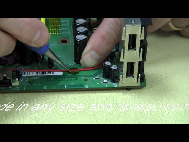
This video demonstrated the use of BEST Inc HotDots(TM) which allow wires to be affixed to the PCB or other surfaces-even when those surfaces go through reflow. There are other similar products out there but none of which can be readily customized no

This video describes the J-STD-001 solder certification program. It is an overview of the program, the certification requirements and the types of credentials. For More Information On IPC J-STD-001 Training Visit Our Website: IPC J-STD-001 CIT Cert
Training Courses | | | PCB Design Courses
The PCB design courses teach students the process, techniques and tools needed to design layout of printed circuit boards.
Training Courses | | | PCB Assembly Courses
The PCB assembly courses provide knowledge of different processes and equipment used in TH and SMT assembly of printed circuit boards.
Events Calendar | Wed Mar 17 18:30:00 UTC 2021 - Wed Mar 17 18:30:00 UTC 2021 | ,
India Chapter Webinar: PCBA Process Qualifications
Events Calendar | Sun Jun 09 18:30:00 UTC 2024 - Sun Jun 09 18:30:00 UTC 2024 | Carlsbad, California USA
San Diego Chapter In-Person Event: IPC J-STD-001 Compliant Solder Pattern Calculations for DFA
Career Center | Clarksburg, Maryland USA | Engineering,Management,Research and Development,Technical Support
We are currently seeking a Senior Manufacturing Engineer for our Clarksburg, Maryland location. The candidate must be driven with a strong ability to multi-task under pressure. Responsibilities: The successful candidate will be responsible for:
Career Center | San Jose, CA, California USA | Engineering,Production,Research and Development
Senior PCB Designer: Want to be part of an exciting pre-IPO enterprise B2B company working on the cutting edge of internet-of-things, artificial intelligence & agents, blockchain, and manufacturing technology? This well-funded venture-backed co
Career Center | Newport Beach, California USA | Engineering,Management,Production
KEVIN RAGER P.O.BOX 7878, NEWPORT BEACH, 949 922 8997, KEVIN.RAGER@EDA-INC.US OBJECTIVE I am trying to find a consistent work flow that provides mentally challenging yet stimulating experiences in design and prototype development. EXPERIENCE 1997
Career Center | reston, Virginia USA | Engineering,Management,Production,Technical Support
NIGEL COOMBER (703 715 1075) email: ncoomber@yahoo.com OBJECTIVE: To contribute in a position of high responsibility for a progressive technically innovative company which can utilize a highly motivated professional with leading edge experience in a
| https://www.eptac.com/blog/3-common-pcb-design-mistakes
3 Common PCB Design Mistakes Looking for solder training standards, manuals, kits, and more? Visit soldertraining.com Training Training Materials Locations Resources Ask Helena
PCB Libraries, Inc. | https://www.pcblibraries.com/forum/topic43&OB=DESC.html
Mask opening for 0201 parts - PCB Libraries Forum Forum Home > Libraries > Footprints / Land Patterns > Expedition New Posts FAQ Search Events Register Login Mask opening for 0201 parts
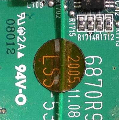
 – pn 51305433.jpg)
 51305434_1.jpg)


