
Industry Directory | Consultant / Service Provider / Manufacturer / Other
ScanCAD is an industry leader in inspection, measurement, process control and reverse engineering. Our solutions support OEM's, manufacturers, stencil fabricators, repair depots, and others in optimizing quality and yield.

Industry Directory | Consultant / Service Provider / Media / Publisher / Online Resource / Other
PCB Libraries' "Footprint Expert" suite uses CAD LEAP(tm) Technology to greatly simplify footprint and 3D STEP model creation; it is used by tens of thousands of PCB designers and engineers all over the world.

We are well versed in the following thermal application materials: Sil-Pad thermally conductive insulators Gap-Pad thermally conductive gap filling material Q-Pad thermal grease replacement film Bond-Ply thermally conductive adh

The PCB Footprint Expert is a powerful CAD library development tool powered by our own proprietary CAD LEAP Technology (Libraries Enhanced with Automated Preferences). It is packed with very powerful advanced library management features that cuts foo
Electronics Forum | Fri Jan 06 05:03:11 EST 2012 | richieoreilly
Hi All, Just wondering if anyone is placing 0201 components in volume. If so What pad layout are you using, i.e. pad size, shape and spacing. Also are you pads and fiducials solder mask defined or copper defined. Can you also let me know the rough q
Electronics Forum | Fri Jan 06 13:47:15 EST 2012 | davef
Your starting [and finishing] point should be IPC-7351B Land Pattern Calculator and Tools - http://landpatterns.ipc.org/default.asp For more, look here: * http://www.smtnet.com/bob-willis/pbdai.html * http://www.onboard-technology.com/pdf_novembre
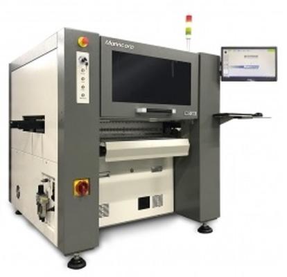
Used SMT Equipment | Pick and Place/Feeders
MC389CY-F3-V MC-389 High-Speed, High-Mix Pick & Place WITH CONVEYOR Heavy-duty, welded steel base frame w/ adjustable foot pads High-precision ball screw X-Y drive mechanism w/ linear encoders Three pick and place heads, each with servo-drive
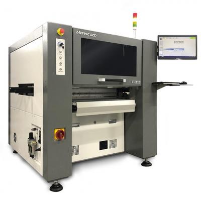
Used SMT Equipment | Pick and Place/Feeders
Heavy-duty, welded steel base frame w/ adjustable foot pads High-precision ball screw X-Y drive mechanism w/ linear encoders Three pick and place heads, each with servo-driven Z- and ?-axis motors Standard on-the-fly vision alignment cameras for c
Industry News | 2011-09-12 12:04:25.0
GPD Global will showcase its Positive Cavity Displacement (PCD) 'H' Series high-resolution pumps in Booth #439 at the upcoming IMAPS 44th International Symposium on Microelectronics
Industry News | 2011-11-20 13:36:13.0
GPD Global has been awarded two Global Technology Awards in the categories of Adhesives/Coatings/Encapsulants and Dispensing Equipment for its PCD Dispensing on the MAX Series Platform
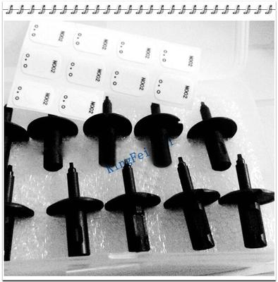
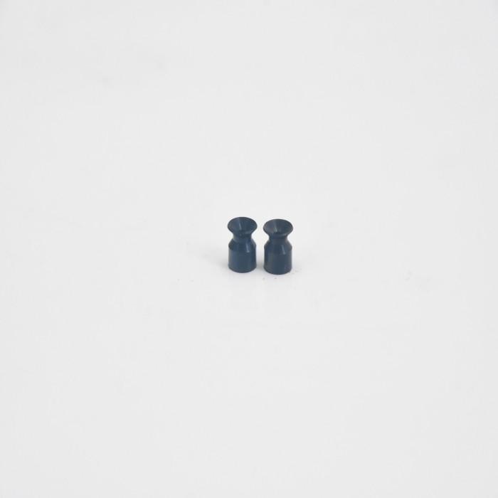
Parts & Supplies | Assembly Accessories
M001 I-PULSE Nozzle M2 PK NZ -N001 (0.5 X 0.4)mm N002 I-PULSE Nozzle M2 PK NZ -N002 (0.9 X 0.62) N003 I-PULSE Nozzle M2 PK NZ -N003 (1.3 X 0.7) N004 I-PULSE Nozzle M2 PK NZ -N004 (1.8 X 1.2) N005 I-PULSE Nozzle M2 PK
Parts & Supplies | Pick and Place/Feeders
Panasonic PAD 1403 KXF08C8AA00 Introducing the Panasonic PAD 1403 KXF08C8AA00, now available at QYSMT, the leading provider of top-of-the-line SMT machines and parts. This product is 100% original and new, ensuring reliability and longevity for y
Technical Library | 2023-05-02 19:03:34.0
The demand for 0201 components in consumer products will increase sharply over the next few years due to the need for miniaturization. It is predicted that over 20 billion 0201 components will be used in more than one billion cell phones worldwide by the year 2003. Therefore, research and development on 0201 assembly is becoming a very hot topic. The first step to achieve a successful assembly process is to obtain a good PCB design for 0201 packages. This paper presents the data and criteria of PCB design for 0201 packages, including the pad design for 0201 components, and the minimum pad spacing or component clearance between 0201 components or between 0201 and other components. A systematic study on pad design and pad spacing was undertaken, using two test vehicles and three Design of Experiments (DOEs). In the first DOE, 2 out of 18 types of 0201 pad designs were selected based on process yield. The second DOE was focused on pad spacing, including 10mil, 8mil, 6mil and 4mil. The third experiment was final optimization, using two types of optimized pad designs with 10mil, 8mil and 6mil pad spacing. Through the above experiments, the design guideline for PCB layout for 0201 packages and the assembly process capability are identified.
Technical Library | 2019-05-29 01:47:22.0
1.Vias near SMD pads: Solder can flow into the via after melted. As a result cold joint will appear in the end. Check the picture below. 2.Vias on SMD pads: Solder can flow into the via more easier after melted. Check the picture below. 3.Via opening without soldermask covered. When workers solder TH parts by hand, soldering iron can touch vias sometime, then tiny amounts molten solder will stay on vias. This can lead to electrical short easily. We recommend you make all vias tenting (covered by solder mask) if it is possible.
PCBNPI-Professional PCB Fab/PCB Assembly Service Provider From China

www.unisoft-cim.com/pcbtest.htm - In minutes the Unisoft ProntoTEST-FIXTURE software translates CAD & BOM files into real reference designators, netlists, X/Y component pin geometries, values, tolerances, part numbers, etc. This data is used by Test

The PCB Footprint Expert is a powerful CAD library development tool powered by our own proprietary CAD LEAP Technology (Libraries Enhanced with Automated Preferences). It is packed with very powerful advanced library management features that cuts foo
Training Courses | | | PCB Rework and Hand Soldering Courses
The PCB rework and hand soldering courses courses cover techniques of rework and repair of PCBs, BGAs and other electronics assemblies, and teach fundamentals of soldering of electronics assemblies.
Training Courses | | | PCB Rework and Hand Soldering Courses
The PCB rework and hand soldering courses courses cover techniques of rework and repair of PCBs, BGAs and other electronics assemblies, and teach fundamentals of soldering of electronics assemblies.
Events Calendar | Wed May 31 00:00:00 EDT 2023 - Wed May 31 00:00:00 EDT 2023 | Holtsville, New York USA
Long Island Chapter Meeting: Fine Feature Paste Printing, Stencil Design and Solder Technology
Events Calendar | Thu Mar 18 00:00:00 EDT 2021 - Thu Mar 18 00:00:00 EDT 2021 | ,
India Chapter Webinar: PCBA Process Qualifications
Career Center | Sherman, Texas USA | Engineering,Production,Research and Development,Technical Support
SMT Packaging Engineer: Location: Texas - Sherman , TX Group: HVAL Degree Requirements: BS ME/ChemE/Materials The person in this position will have the ability to make very significant financial contributions to TI because this is a very critic
Career Center | Lincoln, Nebraska USA | Engineering
Brief Description of Job Duties: Provide new program engineering support with emphasis on technical SMT process development. Key activities would include recommendations and implementation of components, SMT pad design, solder methods, testing and r
Career Center | Bangalore, India | Engineering,Maintenance,Production,Technical Support
SMT Stencil designing & Knowledge of full SMT process software known CAD/CAM -circuit CAM Pro 7.3,GC Power station, GCCAM Edit,Auto CAD, Fault finding of Electronic Boards & Servicing electronic machines.
Career Center | Newport Beach, California USA | Engineering,Management,Production
KEVIN RAGER P.O.BOX 7878, NEWPORT BEACH, 949 922 8997, KEVIN.RAGER@EDA-INC.US OBJECTIVE I am trying to find a consistent work flow that provides mentally challenging yet stimulating experiences in design and prototype development. EXPERIENCE 1997
PCB Libraries, Inc. | https://www.pcblibraries.com/forum/design-smt-pad-for-magnet-wire_topic1206.html
Design SMT pad for magnet wire - PCB Libraries Forum Forum Home > PCB Footprint Expert > Questions & Answers New Posts FAQ Search Events Register Login Design SMT pad for magnet wire
Imagineering, Inc. | https://www.pcbnet.com/blog/considerations-for-pcb-board-design-layout/
Considerations for PCB Board Design & Layout | Imagineering, Inc. Skip to main content Resources Support Contact Us FAQs Live Chat My Account 847-806-0003 Menu PCB Capabilities Fabrication Technology Roadmap Materials Available HDI Tolerances Certifications