Industry Directory | Other / Consultant / Service Provider / Manufacturer
ScanCAD is an industry leader in inspection, measurement, process control and reverse engineering. Our solutions support OEM's, manufacturers, stencil fabricators, repair depots, and others in optimizing quality and yield.
Industry Directory | Manufacturer
We manufacture and market stencil rolls for the PCBA industry. The cleaning material is ideal for cleaning stencils with fine pitch apertures. It prevents smearing, solder balls and other problems on the PC boards. Our stencil product is of high g
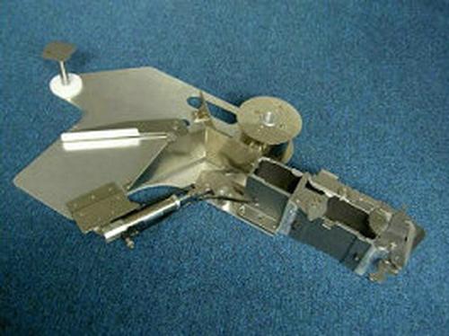
New Equipment | Solder Paste Stencils
Miniature SMT Rework Stencils are laser cut solder paste stencils designed to replicate the intial manufacturing process albeit for a designated component or select area. These laser cut mini stencils can either have flaps (to prevent neighboring are
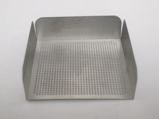
New Equipment | Solder Paste Stencils
SMT Prototype Stencils are laser cut solder paste prototype stencils designed to work on their own for hand printing. These laser cut prototype stencils do not need to be permanently glued in a frame. These so-called framelessstencils are less expens

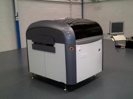
Used SMT Equipment | Screen Printers
DEK Horizon 03i automatic stencil printer Specification : DEK Horizon 03i High Precision Automatic Solder Paste Printer designed for high precision steel mesh printing or stencil printing in SMT industry. Printing PCB size: 50x50mm to 508x510mm;
Used SMT Equipment | Screen Printers
DEK 03iX Specs: • Process alignment capability 2 Cpk @ ± 25µm 6-Sigma • Machine alignment capability 2 Cpk @ ± 12.5µm 6-Sigma • 12 second cycle time • High Throughput Conveyor (option) , enables core cycle time reduction to just 11 seconds • DE
Industry News | 2003-03-21 08:12:24.0
Tecan reckons it is consistently producing what may be regarded as the most efficient stencils in the world today.
Industry News | 2016-02-27 20:41:52.0
BEST Inc. instructors will be conducting 2 training sessions this year at the APEX Expo 2016 - Advanced Rework: Hands-on BGA Reballing, Lead-Free Devices, and Fine-Pitch Parts, and the 2nd session - Stencil Printing: Consistent Print Volumes for SMT Rework.
Technical Library | 2023-07-25 16:25:56.0
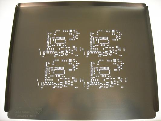
This paper address two significant applications of stencils in advance packaging field: 1. Ultra-Thin stencils for miniature component (0201m) assembly; 2. Deep Cavity stencils for embedded (open cavity) packaging. As the world of electronics continues to evolve with focus on smaller, lighter, faster, and feature-enhanced high- performing electronic products, so are the requirement for complex stencils to assemble such components. These stencil thicknesses start from less than 25um with apertures as small as 60um (or less). Step stencils are used when varying stencil thicknesses are required to print into cavities or on elevated surfaces or to provide relief for certain features on a board. In the early days of SMT assembly, step stencils were used to reduce the stencil thickness for 25 mil pitch leaded device apertures. Thick metal stencils that have both relief-etch pockets and reservoir step pockets are very useful for paste reservoir printing. Electroform Step-Up Stencils for ceramic BGA's and RF Shields are a good solution to achieve additional solder paste height on the pads of these components as well as providing exceptional paste transfer for smaller components like uBGAs and 0201s. As the components are getting smaller, for example 0201m, or as the available real estate for component placement on a board is getting smaller – finer is the aperture size and the pitch on the stencils. Aggressive distances from step wall to aperture are also required. Ultra-thin stencils with thicknesses in the order of 15um-40um with steps of 15um are used to obtain desired print volumes. Stencils with thickness to this order can be potential tools even to print for RDLs in the package.
Technical Library | 2017-09-28 16:36:33.0
These nano-coatings also refine the solder paste brick shape giving improved print definition. These two benefits combine to help the solder paste printing process produce an adequate amount of solder paste in the correct position on the circuit board pads. Today, stencil aperture area ratios from 0.66 down to 0.40 are commonly used and make paste printing a challenge. This paper presents data on small area ratio printing for component designs including 01005 Imperial (0402 metric) and smaller 03015 metric and 0201 metric chip components and 0.3 mm and 0.4 mm pitch micro BGAs.
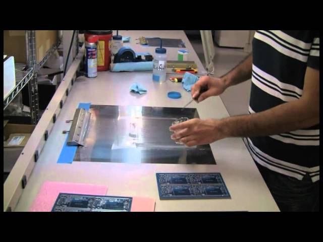
This is video shows how to print a PCB using a prototype foil only stencil. The SMT prototype stencil (www.soldertools.net) is made from a high nickel content material able to offer repeatable high precision apertures. The steps of alignment, printin
This is video shows how to print a PCB using a prototype foil only stencil. The SMT prototype stencil (www.soldertools.net) is made from a high nickel content material able to offer repeatable high precision apertures. The steps of alignment, printin
Events Calendar | Mon Dec 07 18:30:00 UTC 2020 - Mon Dec 07 18:30:00 UTC 2020 | Online,
SMTA California Technology Day
Events Calendar | Tue May 30 18:30:00 UTC 2023 - Tue May 30 18:30:00 UTC 2023 | Holtsville, New York USA
Long Island Chapter Meeting: Fine Feature Paste Printing, Stencil Design and Solder Technology
Career Center | Lumberton, New Jersey USA | Engineering
Reports to: Cad/Laser Manager Department: Cad Location: Lumberton Phone: 609-261-2670 Ask for Greg Starrett Email: Send resume as a word document or PDF to greg@metassocs.com Job Summary: Under the general supervision of the Cad Manager
Career Center | rochester, New York USA | Engineering
Skill Set . ASQ: Certified Six Sigma Green Belt (CSSGB) (Appearing 12/01/2007) . SMT Process Related Skills . Stencil Printing . Reflow Profiling . Selective Soldering . Rework . RSlogix � Programmable Logic Controller . Minitab 15.1 . Arena - Manu
Career Center | Chennai, Tamil Nadu India | Engineering,Maintenance,Production,Research and Development,Technical Support
Over 5.5 years exp in Customer service on SMT Roles and Responsibilities Identify, improve, recommend, and implement measures to improve production methods, equipment performance, process capability, and product quality. Streamline manufac
SMTnet Express, April 16, 2020, Subscribers: 35,920, Companies: 10,989, Users: 25,757 Stencil Printing 008004/0201 Aperture Components Credits: ITW EAE This paper will focus on the application requirements of solder printing small aperture designs
SMTnet Express, September 2, 2021, Subscribers: 26,737, Companies: 11,436, Users: 26,825 Tombstoning Of 0402 And 0201 Components: "A Study Examining The Effects Of Various Process And Design Parameters On Ultra-Small Passive Devices
| http://etasmt.com/cc?ID=te_news_industry,24564&url=_print
. Consider adjusting the stencil aperture size when printing. Keywords : Check Our Youtube SMT Reflow Oven , Nitrogen Reflow Oven , Dual Lane Reflow Oven , Vertical Reflow Oven , Vacuum SMT Reflow Oven , Lead free SMT Reflow Oven , Reflow Oven Manufacturer , LED Reflow
Heller Industries Inc. | https://hellerindustries.com/opensor-insufficient-solder/
stencil aperture Misaligned solder print Improper stencil thickness Inadequate stencil aperture size Excessive pad size Via in pad draining solder from interconnection Reflow-related causes of