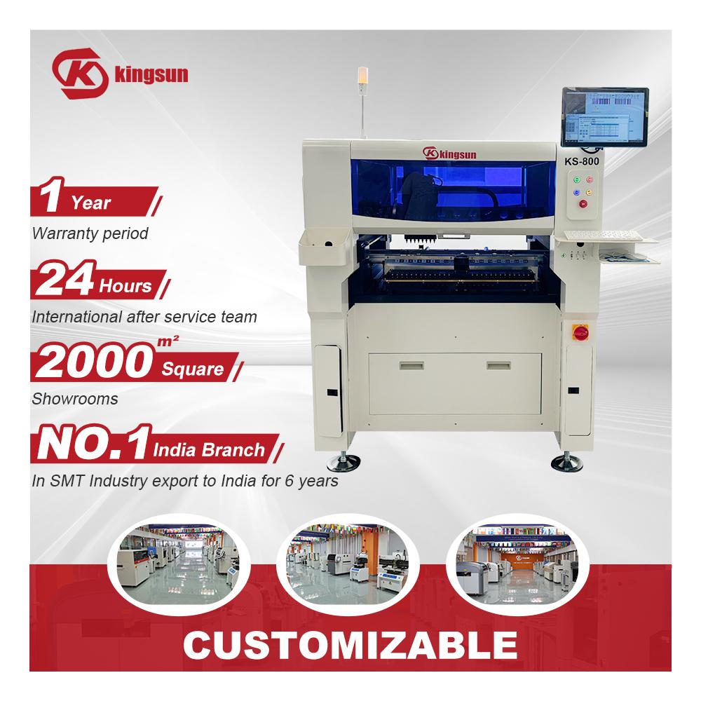
KS-800 New High-precision multi-functional LED SMT Pick and Place Machine, eight head in one take and stick, low energy consumption; independent research and development of integrated light weight,all 8 sets of Z-axis are controlled by independent mo
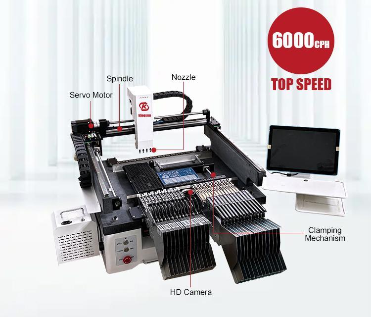
KS-2425Z4 desktop SMT pick and place machine is a current market fastest actual mounting speed, the most stable performance and the best quality equipment. With marble mounting platform, 4 Heads +56 Feeder stations in one take and stick, support pneu
Electronics Forum | Thu Oct 20 10:31:27 EDT 2011 | ck_the_flip
What is the industry standard pad geometry (dimensions and spacings) for 0402 components?
Electronics Forum | Wed Jun 12 10:42:06 EDT 2002 | stepheno
Check your land patterns. I believe someone once made a typo on specs for land pattern spacing and the specs are still being used by some people. I worked for a CM that had a customer that spaced the pads for 0402's too far apart. It was the only
Used SMT Equipment | Pick and Place/Feeders
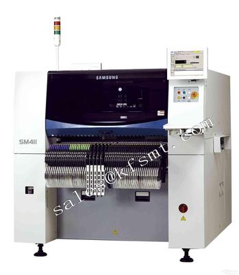
Samsung SM411, Samsung SM411 Mounter, Second-hand Samsung SM411 Chip Shooter Equipment Profile: The SM411 uses the Samsung Patent On The Fly identification method and the double cantilever structure to achieve the chip component 42,000 CPH an
Used SMT Equipment | Pick and Place/Feeders
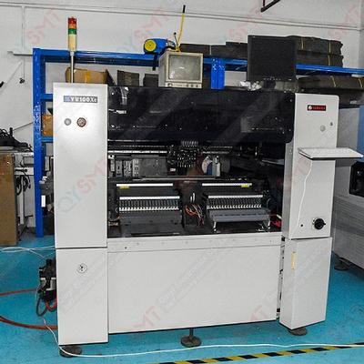
Yamaha YV100X parameters Substrate size ATS20 (end orientation) W-AT assembly: L460*W250(Max)/L50*W50(Min) Substrate thickness 0.4-3.0 SMD components can be placed 100 kinds (8MM) Board transfer direction right-left Mounting accuracy ±0.1m
Industry News | 2014-01-16 09:31:26.0
The increased challenge of miniaturization with increased functionality within the PCB industry leads to the constant need for new technologies for high volume manufacturing. As line and space features decrease, requirements on the photoresist as well as its pre-treatment steps increase.
Industry News | 2003-02-14 08:03:50.0
Provides Devices with Excellent Protection Against EMI and Overcomes Limitations of Metal Cans
Parts & Supplies | Assembly Accessories
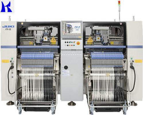
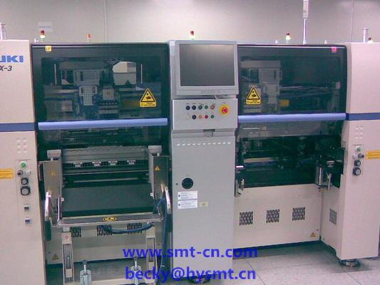
SMT JUKI High-speed Modular Mounter FX-3 with better price now JUKI HIGHT SPEED SHOOTER KE2050 KE2060 KE2070 KE2080 KE1070 KE1080 FX-1R FX-2 FX-3 Sell & Buy smt machine and spare parts. Pls don't hesitate to contact me if you have any requi
Parts & Supplies | Pick and Place/Feeders
Starting in May 2008, JUKI Corporation (President Kazuyuki Nakamura; listed on First Section of the Tokyo Stock Exchange) is beginning worldwide sales of its High-speed Modular Mounter FX-3. The FX3 is an industrial robot for mounting electronic comp
UV Laser PCB Depaneling System, Dual Table for High Volume Laser Depaneling Purpose: The processing and application objects are PCB, FPC soft and hard plate and related material cutting, cover opening and other operations. Efficient integration
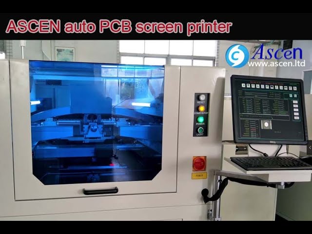
https://www.ascen.ltd/Products/Solder_paste_printer/513.html full auto PCB screen printer and SMT solder paste printing machine with Image and optical system,It is a very accurate fully automatic SMT stencil printer.automatic PCB screen printer main
GPD Global | https://www.gpd-global.com/co_website/pdf/doc/FLOware-Software-Guide-Addendum-Deferred-Reverse.pdf
Description 7/12/19 GPD Global® 13 Servo Pump Deferred Reverse References Fill Width The wall dimension (the width of each side) of a hollow rectangle. The pattern is covered in increments of Fill Spacing needle diameters and motion is at vector speed Dispense
| https://unisoft-cim.com/crosschecking-pcb-component-footprint-and-bom-footprint.html
(correct solder pad size and land pattern) for the same component listed in the Bill of Materials (BOM). The mismatch of component footprint spacing is usually an error created when components on the PCB assembly ( PCBA


