Industry Directory | Consultant / Service Provider
PCB assembly services, both US and offshore. We handle basic through-hole to standard surface mount to ultra-fine pitch. Quote and order PCB fabrication and assembly online.
New Equipment | Soldering - Other
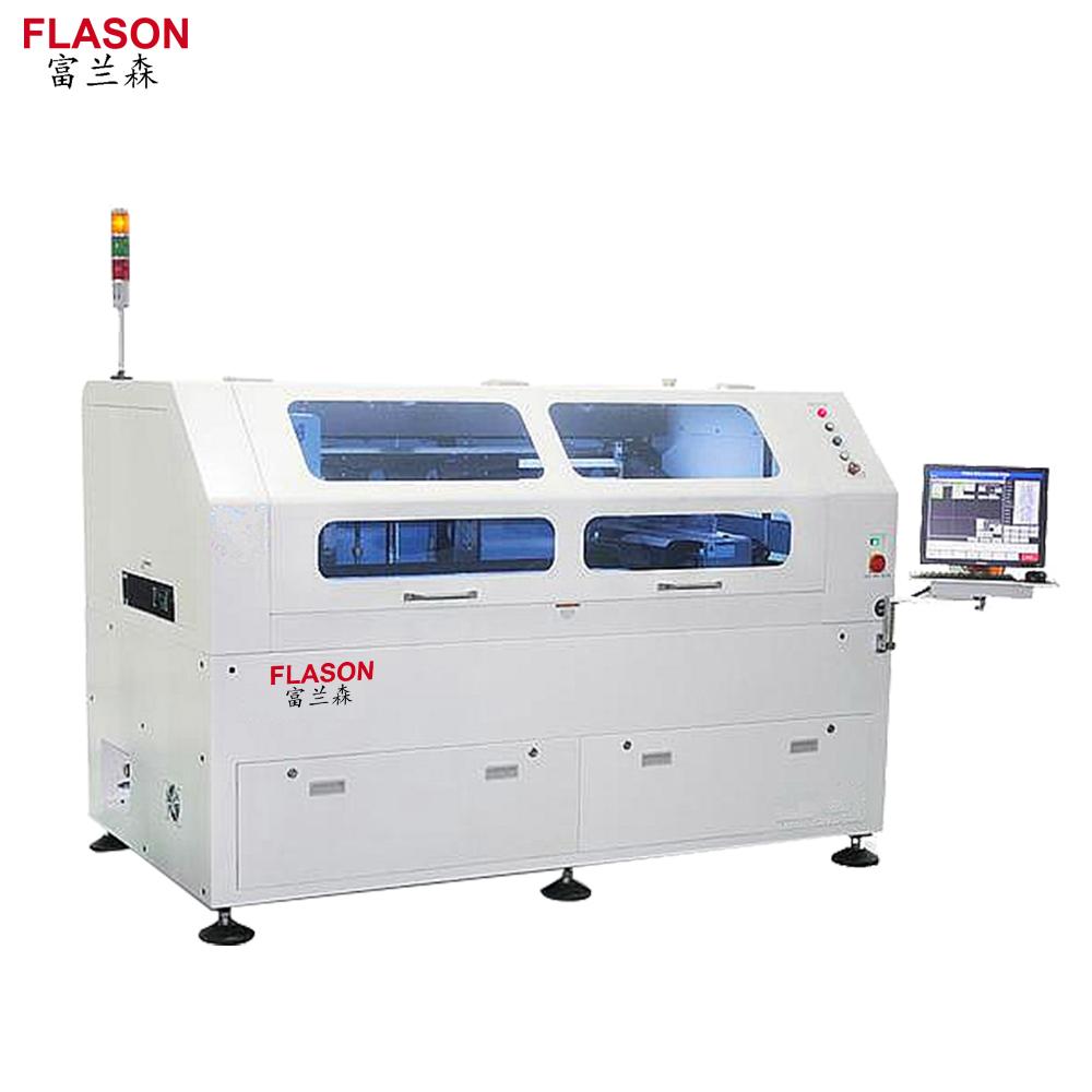
SMT Stencil Printer Automatic 1200mm Solder paste printer for SMT assembly line Power Supply: AC:220±10%,50/60HZ Control Method: PC Control PCB Size/Max:1200*340mm Weight Approx:1500Kg Product description: Automatic1200mm So
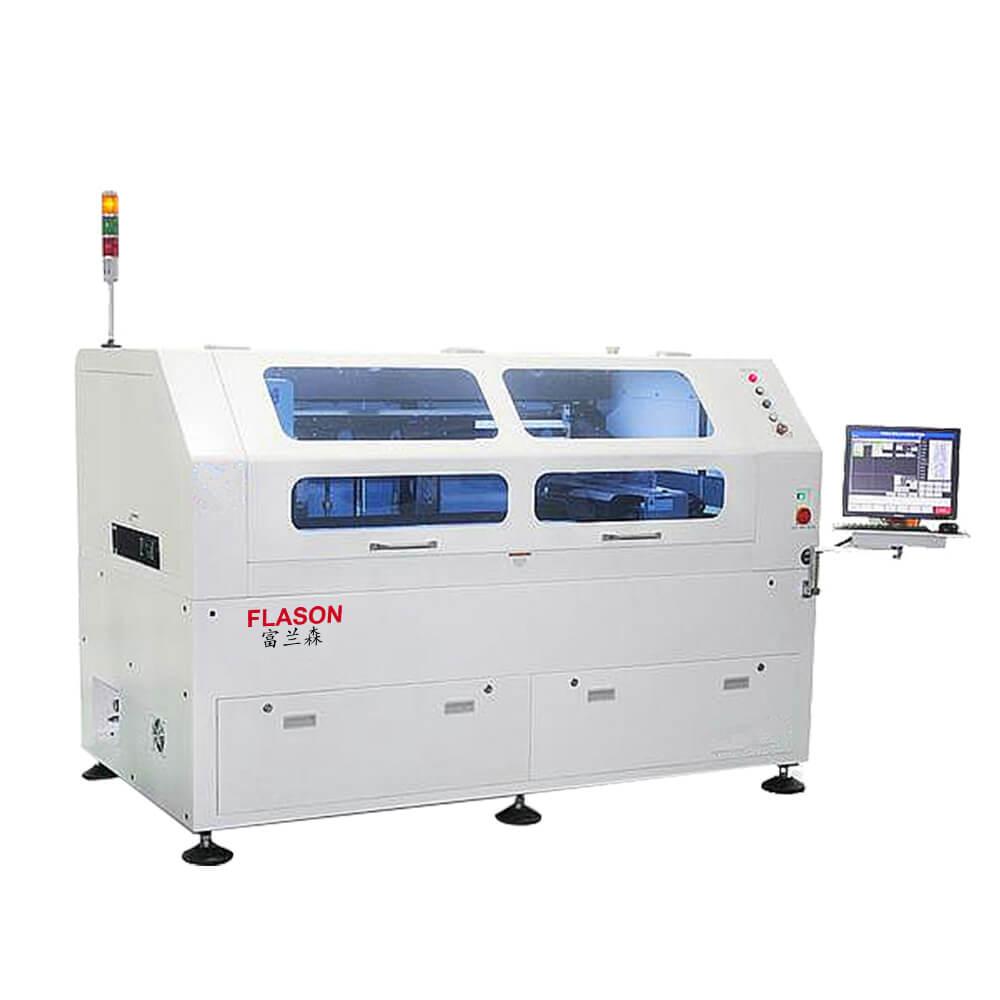
Flason SMT Automatic SMT 1200mm Solder paste printer for SMT assembly line Power Supply: AC:220±10%,50/60HZ Control Method: PC Control PCB Size/Max:1200*340mm Weight Approx:1500Kg Product description: Automatic1200mm SMT Solder paste p
Industry News | 2018-10-18 08:14:11.0
How to Prevent the Tombstone and Open Defects during the SMT Reflow Process
Industry News | 2018-10-18 08:32:52.0
How to Prevent Solder Ball and Bridging Defects during the SMT Reflow Process
Technical Library | 2015-05-28 17:34:48.0
The printed circuit board assembly industry has long embraced the "Smaller, Lighter, Faster" mantra for electronic devices, especially in our ubiquitous mobile devices. As manufacturers increase smart phone functionality and capability, designers must adopt smaller components to facilitate high-density packaging. Measuring over 40% smaller than today's 0402M (0.4mmx0.2mm) microchip, the new 03015M (0.3mm×0.15mm) microchip epitomizes the bleeding-edge of surface mount component miniaturization. This presentation will explore board and component trends, and then delve into three critical areas for successful 03015M adoption: placement equipment, assembly materials, and process controls. Beyond machine requirements, the importance of taping specifications, component shape, solder fillet, spacing gap, and stencil design are explored. We will also examine how Adaptive Process Control can increase production yields and reduce defects by placing components to solder position rather than pad. Understanding the process considerations for 03015M component mounting today will help designers and manufacturers transition to successful placement tomorrow.
Technical Library | 2023-05-02 18:50:24.0
Surface-mount PCB components are smaller than their lead-based counterparts and provide a radically higher component density. They are available in a variety of shapes and sizes designated by a series of standardized codes curated by the electronics industry. Of these PCB components, the 0201-sized are the smallest, measuring 0.024 x 0.012 in. (0.6 x 0.3 mm) – that's 70% smaller than the previous 0402 level! The 0201 components are designed to improve reliability in space-constrained applications such as portable electronics like smartphones, tablets, robotics and digital cameras, but require delicate handling during the assembly process. Given the miniaturized dimensions of an 0201 package, it is crucial that the mounting process abide by a series of guidelines regarding the design of the PCB mounting pads and solderable metallization, PCB circuit trace width, solder paste selection, package placement and overages, solder paste reflow, solder stencil screening, and final inspection. It's advisable that one review this information when procuring the services of a PCB assembler.
Using Hansen Space to Optimize Solvent Based Cleaning Processes for Manufacturing Electronic Assemblies News Forums SMT Equipment Company Directory Calendar Career Center Advertising About FREE Company Listing! Using Hansen Space
ORION Industries | http://orionindustries.com/pdfs/silpad400.pdf
. Special Thicknesses, Rolls and Sheets Sil-Pad 400 can be supplied on special order in a variety of thicknesses from .007 to .045 inches to fulfill special requirements of insulation path minimums or other spacing needs
GPD Global | https://www.gpd-global.com/co_website/fluid-dispense-solderpaste-dispenser.php
: Solder Paste Dots, Lines, Complex Shapes, 01005, 0402 Solder Paste is used to make electrical connection between a PCB and component


