Eclipse Industries manufactures the ultra-high precision DS-107 Aligner Bonder, alignment to 1-2 microns, bond force 5 gm to 100 kg. Applications are flip chip, die bonding, CSP, uBGA, MCM, flat panel displays, die-to-wafer & optoelectronics.

The eP33/eP35 employs a number of unique features to provide fast and accurate deposition of solder paste within +/- 12 microns, namely: A heavy-duty, mono-block casting, enabling optimal mechanical rigidity. A precision, two-stage servo-driven gran
As population of circuit boards become more dense and with continual component size reductions, printing precision has become more challenging. Not only are improvements necessary to the manufacturing equipment & process, but also its raw material se
Electronics Forum | Wed Sep 03 16:15:30 EDT 2008 | blnorman
Elemental is by SEM/EDX. The brown coloration does resemble the 3 micron photo. Again, if I'm picking up copper (our Ag plating thickness requirements are 0.05 micron to 0.12 micron following IPC 4553), maybe we do have a porous silver plating.
Electronics Forum | Mon Apr 22 17:13:48 EDT 2013 | hegemon
Might want to double check my figures, but my notes have 2oz copper at 2.8 mils or 71.12 microns in thickness. 'hege
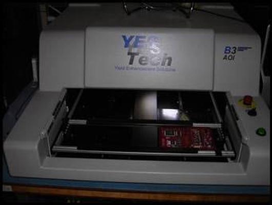
Used SMT Equipment | AOI / Automated Optical Inspection
Make: Yestech Model: B3 Vintage: 2008 Details: • Green Lighting • Thin Camera: 25 Micron and 12 Micron Pixel Size • Operating System Windows XP • Software 2.7.7 Condition: Complete and Operational “As is Where is” (can be seen under power)
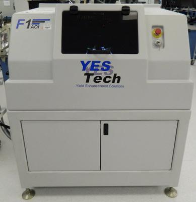
Used SMT Equipment | AOI / Automated Optical Inspection
Make: Yestech Model: YTV F1S Vintage: 2007 Details: • High Magnification Camera (12 Micron) 0201 • Conveyor Board Clamp Kit • Pneumatic Support Kit • Offline Programming and Defect Support Software Condition: Available for inspection prior to
Industry News | 2012-06-01 13:55:57.0
As chip speeds skyrocket and system sizes diminish, designers and manufacturers face new and complex challenges
Industry News | 2001-10-30 07:31:00.0
Hoping to extend its lead in DRAMs and other chip products, South Korea's Samsung Electronics Co. Ltd. here today announced that it has begun mass production in its initial 300-mm wafer fab.
Technical Library | 2009-07-22 18:33:41.0
This paper deals with the thermal effects of joule heating in a high interconnect density, thin core, buildup, organic flip chip substrate. The 440 μm thick substrate consists of a 135 μm thick core with via density of about 200 μm. The typical feature sizes in the substrate are 50 micron diameter vias is the core/buildup layers and 12 micron thick metal planes. An experimental test vehicle is powered with current and the temperature rise was measured. A numerical model was used to simulate the temperature rise in the TV.
Baja Bid | https://bajabid.com/product/nordson-yestech-bx-benchtop-aoi/
: https://www.dropbox.com/sh/qv57qmmuig2nkrj/AABep6-b3xavybHz07DKBJu_a?dl=0 Specifications: High Resolution Full Color CCD All Digital 12 micron optics plus Adjustable PCB
QYSMT SOLUTION USA LLC / Qinyi Electronics Co.,Ltd | https://www.qy-smt.com/shop/4-719-920-01-ball-rope-dia-2-0-micron-182599?page=106&order=name+asc
SONY BALL, ROPE (DIA 2+-0 MICRON*) 4-719-920-01 | QYSMT × Home about Us ABOUT US FAQ SMT spare parts SMT surplus equipment SMT peripheral equipments News Contact US 0 0 Sign in contact us Products BALL, ROPE (DIA 2+-0 MICRON