The ASTE ( a all volunteer non-profit corporation) is dedicated to the Quality, Integrity, and Advancement of the Test Engineering Profession, Peer Helping Peer. Visit us at www.astetest.org
Electronics Forum | Wed Oct 13 06:20:00 EDT 2010 | costache
Dear All > > I need to check the solder paste > volume inside the PTH at our board,which size is > 440x620 mm.So, I may need 3D inspection > machine,AXI, not AOI.So, does anyone recommand me > which 3D machine is suited to my PCB? Thanks in > a
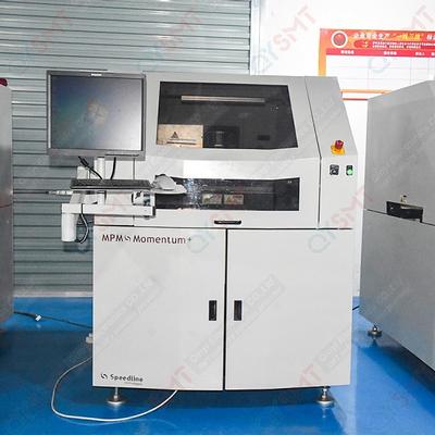
Used SMT Equipment | Screen Printers
Substrate processing: Maximum substrate size (XxY): 609.6mmx508mm(24”x20”) For circuit boards larger than 20”, special fixtures are required Minimum substrate size (XxY): 50.8mmx50.8mm(2”x2”)
Industry News | 2008-03-24 22:56:01.0
Agilent Technologies Inc. (NYSE: A) today announced that its Protocol Test Card (PTC) 2.0 has been approved by the PCI-SIG(r) (PCI Special Interest Group) for PCI Express(r) (PCIe(r)) 2.0 protocol testing. This approval means designers can use Agilent's PTC 2.0 to test and validate their designs with the confidence that the PCIe specifications for link layer, transaction layer and BIOS are being met.
Industry News | 2007-11-08 21:29:06.0
Agilent Technologies Inc. (NYSE: A), the provider of the gold standard Protocol Test Card I (PTC I), today introduced the PTC II for PCI Express(r) (PCIe(tm)) 2.0. The Agilent PTC II will enable device compliance with the PCI-SIG(r) (PCI Special Interest Group) specifications and industry deployment of PCIe by providing all the mandatory test cases.
Substrate processing: Maximum substrate size (XxY): 609.6mmx508mm(24”x20”) For circuit boards larger than 20”, special fixtures are required Minimum substrate size (XxY): 50.8mmx50.8mm(2”x2”)
Training Courses | | | ESD Control Training Courses
Browse training and certification programs for electrostatic discharge (ESD) control in electronics assembly.


