Industry Directory | Distributor
Used X-ray Machine Brand: Creative Electron. Model: TruView Prime, SB-80-500
High Precision Dispensers - MAX Series (Non-Heated) Max Series is capable of a wide variety of dispense applications including MicroVolume, Solder Paste and Conductive Adhesive, Underfill, Surface Mount Adhesive, Dam and Fill, Encapsulations, LED En
New Equipment | Fabrication Services
PFC designs, manufactures and assembles fine line flex circuits. 50 micon line and space is done in production on a daily basis. 37.5 microns done for prototoypes.
Electronics Forum | Thu Jan 06 15:51:58 EST 2011 | flipit
Indium has it.
Electronics Forum | Wed Jan 05 17:56:30 EST 2011 | ppcbs
I am looking for a No-clean or water soluble solder paste, Sn63/Pb37 alloy, 15 - 25 microns (T5). I need to print with a 4.8 mil stencil opening. Does anyone know where I can get 250 to 500 grams in one week or less?
Used SMT Equipment | Pick and Place/Feeders
Product number: YS88 Products in detail The characteristics of Configurable ~ 0402 chip - 55 mmcomponents, the wide range of special-shaped long joint element The height of the object elementcorresponds to 25.5 mm 10 ~ 30 n can be easy to stick
Used SMT Equipment | SMT Equipment
Product name: YS88 multi-function module chip mounter Product number: YS88 Products in detail The characteristics of Configurable ~ 0402 chip - 55 mm components, the wide range of special-shaped long joint element The height of the object elem
Industry News | 2019-08-21 16:21:55.0
The SMTA will organize the “Additive Electronics Conference: PCB Scale to IC Scale” on October 24, 2019 at the DoubleTree by Hilton San Jose in San Jose, California. The conference examines the manufacturing and design processes enabling line width and space from .003" to 5 microns as well as other new advanced technologies intended to meet the ever-increasing challenges of smaller, lighter and more powerful electronic devices.
Industry News | 2019-09-10 13:38:32.0
The SMTA announced Rich Brooks, Senior Engineering Manager at Jabil Circuit, Inc., will keynote the Additive Electronics Conference on October 24, 2019 at the DoubleTree by Hilton San Jose in San Jose, California.
Parts & Supplies | Assembly Accessories
DEK SMT wiping cylinder (165675) PLEASE CHECK WITH YOUR LOCAL DEK CALL CENTRE. MPU 602137 * 2 MAY BE REQUIRED FOR MICRON OR INST INCTIV MACHINES. GL Applicable models: DEK265/GSX/LT / ELA / HOZ / INF More SMT parts available H1067R A12GD25-1L-
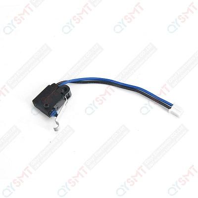
Parts & Supplies | Assembly Accessories
FUJI-sw-micro-PZ02394 electron microscope 3.5-90X Magnification HD HDMI/USB 14MP Camera electron microscope 3.5x-90x stereo microscope MICRO EJECTOR UNIT KM8-M7162-00 MICRO PHOTO SENSOR THETA-AXIS J3212027A J3212027A Micro Switch S5
Technical Library | 2021-09-02 08:17:07.0
We are a professional manufacturer of PCB depaneling machines, which is workable for all boards, including flex and regid boards, v-scored boards and routed boards. Laser pcb depaneling is non-contact way without mechanical stress,this solution is good for modern precision PCB depaneling. It has below advantages: 1. No dust The production environment of the circuit board industry is carried out in the dust-free workshop. The traditional pcb depaneling equipment, such as blade moving type machine, will inevitably produce residues and micro powder, which will pollute the 10000 and 1000 class dust-free workshops and affect the conductivity of products. The UV laser PCB cutting machine is a vaporization processing process, which will not produce dust and is conducive to the conductivity of the product. 2. High cutting precision The processing gap of high-precision traditional processing equipment can not reach the gap width of less than 100 microns, which will cause certain damage to the lines on the edge or PCBA circuit board containing components. The focus spot of the laser cutting machine is small, and the ultraviolet cold processing mode has little thermal impact on the edge of the circuit board. The cutting position accuracy is less than 50 microns, and the cutting size accuracy is less than 30 microns, which will not affect the edge of the circuit board, and the precision is high. 3. No stress Traditional processing methods generally have V-grooves, which will cause certain damage to the board in the manufacturing process. The UV laser PCB cutting machine can directly cut the bare board without making V-grooves. In addition, the traditional processing methods directly use tools to act on the circuit board, especially the stamping method has a great impact on the circuit board, which is easy to cause board deformation. The laser cutting machine is a non-contact processing mode, which acts on the surface of the material through the high-energy beam, which will not cause the influence of stress and the deformation and damage of the circuit board. 4. For special-shaped cutting, it is easy to automate The UV laser PCB cutting machine can cut for any shape without replacing any props and fixtures, and without steel mesh. The same equipment can meet special-shaped and straight-line cutting, which is easy to realize assembly line automatic production and high flexibility. It is easy to improve production efficiency and save production process and production cycle. In particular, it can quickly and efficiently meet the needs of rapid proofing, directly import the drawing, and then locate the cutting. 5. High compatibility The UV laser PCB cutting machine can process the materials around the circuit board, such as PCB, FPC, covering film, pet, reinforcing board, IC, ultra-thin metal cutting, etc. it has strong practicability, is compatible with the processing of a variety of materials, is easy to operate, can be imported into the drawing, does not need to adjust any mechanical parts, and is easy to operate and maintain. 6. Good cutting edge effect The cutting edge is smooth and neat without burr. It can be processed and formed directly according to the size of the drawing, which is conducive to improving the yield of the product. It can be directly installed into the subsequent process without further processing. For more details about UV laser depaneling, please feel free to contact us. www.pcbdepanelingrouter.com
Technical Library | 2020-09-02 22:14:36.0
The demand for miniaturization and higher density electronic products has continued steadily for years, and this trend is expected to continue, according to various semiconductor technology and applications roadmaps. The printed circuit board (PCB) must support this trend as the central interconnection of the system. There are several options for fine line circuitry. A typical fine line circuit PCB product using copper foil technology, such as the modified semi-additive process (mSAP), uses a thin base copper layer made by pre-etching. The ultrathin copper foil process (SAP with ultrathin copper foil) is facing a technology limit for the miniaturization due to copper roughness and thickness control. The SAP process using sputtered copper is a solution, but the sputtering process is expensive and has issues with via plating. SAP using electroless copper deposition is another solution, but the process involved is challenged to achieve adequate adhesion and insulation between fine-pitch circuitries. A novel catalyst system--liquid metal ink (LMI)--has been developed that avoids these concerns and promotes a very controlled copper thickness over the substrate, targeting next generation high density interconnect (HDI) to wafer-level packaging substrates and enabling 5-micron level feature sizes. This novel catalyst has a unique feature, high density, and atomic-level deposition. Whereas conventional tin-palladium catalyst systems provide sporadic coverage over the substrate surface, the deposited catalyst covers the entire substrate surface. As a result, the catalyst enables improved uniformity of the copper deposition starting from the initial stage while providing higher adhesion and higher insulation resistance compared to the traditional catalysts used in SAP processes. This article discusses this new catalyst process, which both proposes a typical SAP process using the new catalyst and demonstrates the reliability improvements through a comparison between a new SAP PCB process and a conventional SAP PCB process.
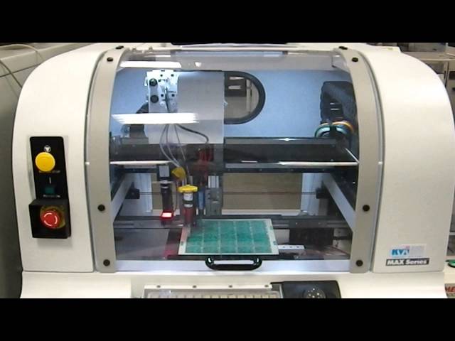
High Precision Dispensers - MAX Series (Non-Heated) Max Series is capable of a wide variety of dispense applications including MicroVolume, Solder Paste and Conductive Adhesive, Underfill, Surface Mount Adhesive, Dam and Fill, Encapsulations, LED En
YAMAHA Mounter-YS12 1) All-round high-precision placement machine; 2) 0.1 second/CHIP ultra-high-speed placement (the best condition is 36000 points/hour); 3) In IPC9850 state, the patch speed is up to 24000CPH; 4) Ensure that the entire plac
Events Calendar | Tue Jan 23 00:00:00 EST 2018 - Tue Jan 23 00:00:00 EST 2018 | Fremont, California USA
Digital X-Ray Inspection Services Open House
Career Center | , California USA | Sales/Marketing
Regaional Sales Manager / Account Manager / Sales Engineer
Career Center | Farrukh Hussain, Pakistan | Engineering,Maintenance
PLC, SCADA, designing circuit or PCB layout, troubleshooting and maintenance, electrical and instrumentation, electronics design, software skill with programming.
| https://pcbasupplies.com/zff-250-filter-5-pack/
» SMT Standard Nozzles » Mycronic & Mydata » Other Consumables » ZFF 250 FILTER (5 PACK) ZFF 250 FILTER (5 PACK) $ 49.00 Purchase this product now and earn 5 Points! ZFF 250 FILTER (5 PACK) quantity — OR — Add to cart Brand
ASYMTEK Products | Nordson Electronics Solutions | https://www.nordson.com/fr-FR/divisions/efd/products/reservoirs-and-pumps/analog-gauge-fluid-reservoirs
réservoir pour dosage direct. Comme les réservoirs sont chargés avec de l'air comprimé, nous recommandons l'emploi d'un filtre/régulateur 5 microns pour filtrer les contaminants


