Industry Directory | Manufacturer
Bones Electronics design and manufacture toroidal transformers,EI lamination transformers,toroidal iron cores wound by sillicon steel tapes. OEM and ODM accept.CE,ROHS,UL,VDE approved.
Industry Directory | Manufacturer
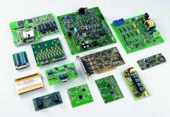
Established on June, 1997, HongTai Technology Co., Ltd is a China-Hong Kong joint venture enterprise, which specializes in PCB, FPC and PCBA.
New Equipment | Assembly Services
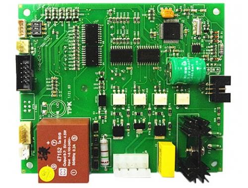
1.ShanXu PCBA Turnkey solution 2.PCB Assembly, PCB/PCBA Design, PCBA Copy 3.Customized PCBA/OEM/ODM/EMS(Electronics Manufacturing Service) 4.SMT&DIP&PTH&BGA Assembly 5.Component sourcing and purchasing 6.Quick PCBA prototyping 7.Test:X-Ray,AOI,
New Equipment | Assembly Services
1.ShanXu PCBA Turnkey solution 2.PCB Assembly, PCB/PCBA Design, PCBA Copy 3.Customized PCBA/OEM/ODM/EMS(Electronics Manufacturing Service) 4.SMT&DIP&PTH&BGA Assembly 5.Component sourcing and purchasing 6.Quick PCBA prototyping 7.Test:X-Ray,AOI,
Electronics Forum | Wed Sep 13 11:23:37 EDT 2006 | teamcanada
Is there any published info on acceptable losses in SMT assembly. Especially for small to medium sized production runs with switch overs several times weekly Different losses for component sizes and packaging? Thx Vaughn
Electronics Forum | Wed Oct 14 03:21:37 EDT 2009 | lincy
We found a PCBA performance have insertion loss at the functional test process. We did some analysis and conclude the main root cause is from the PCB performance. What is the critical parameter in PCB will cause a failure in PCBA frequency performan
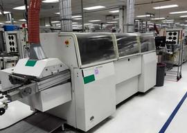
Used SMT Equipment | Soldering - Wave
Windows: XP Version 2002, Service Pack2, KBM Premium Industrial Computer. Vectra Software: Version 3.05.0 Titanium Solder Pot w/ Custom 12” Titanium Ducts/Nozzles (Ultra-Fill & Rotary Chip Wave). Bar Solder Feeder Titanium Solder Pump
Industry News | 2003-04-04 08:46:37.0
Company Announces Further Reductions to Goodwill and Reclassifications of Indebtedness Recorded in Fiscal 2002
.jpg)
Parts & Supplies | Pick and Place/Feeders
Product Description SMT NOZZLE E3503-721-0A0 103 nozzle 1.used in KE2010&2020 2.model: 505 3.Tungsten steel 4.Material loss rate three thousandths Picture Show Model &
Technical Library | 2020-08-27 01:22:45.0
Initially adopted internal specifications for acceptance of printed circuit boards (PCBs) used for wire bonding was that there were no nodules or scratches allowed on the wirebond pads when inspected under 20X magnification. The nodules and scratches were not defined by measurable dimensions and were considered to be unacceptable if there was any sign of a visual blemish on wire-bondable features. Analysis of the yield at a PCB manufacturer monitored monthly for over two years indicated that the target yield could not be achieved, and the main reasons for yield loss were due to nodules and scratches on the wirebonding pads. The PCB manufacturer attempted to eliminate nodules and scratches. First, a light-scrubbing step was added after electroless copper plating to remove any co-deposited fine particles that acted as a seed for nodules at the time of copper plating. Then, the electrolytic copper plating tank was emptied, fully cleaned, and filtered to eliminate the possibility of co-deposited particles in the electroplating process. Both actions greatly reduced the density of the nodules but did not fully eliminate them. Even though there was only one nodule on any wire-bonding pad, the board was still considered a reject. To reduce scratches on wirebonding pads, the PCB manufacturer utilized foam trays after routing the boards so that they did not make direct contact with other boards. This action significantly reduced the scratches on wire-bonding pads, even though some isolated scratches still appeared from time to time, which caused the boards to be rejected. Even with these significant improvements, the target yield remained unachievable. Another approach was then taken to consider if wire bonding could be successfully performed over nodules and scratches and if there was a dimensional threshold where wire bonding could be successful. A gold ball bonding process called either stand-off-stitch bonding (SSB) or ball-stitch-on-ball bonding (BSOB) was used to determine the effects of nodules and scratches on wire bonds. The dimension of nodules, including height, and the size of scratches, including width, were measured before wire bonding. Wire bonding was then performed directly on various sizes of nodules and scratches on the bonding pad, and the evaluation of wire bonds was conducted using wire pull tests before and after reliability testing. Based on the results of the wire-bonding evaluation, the internal specification for nodules and scratches for wirebondable PCBs was modified to allow nodules and scratches with a certain height and a width limitation compared to initially adopted internal specifications of no nodules and no scratches. Such an approach resulted in improved yield at the PCB manufacturer.
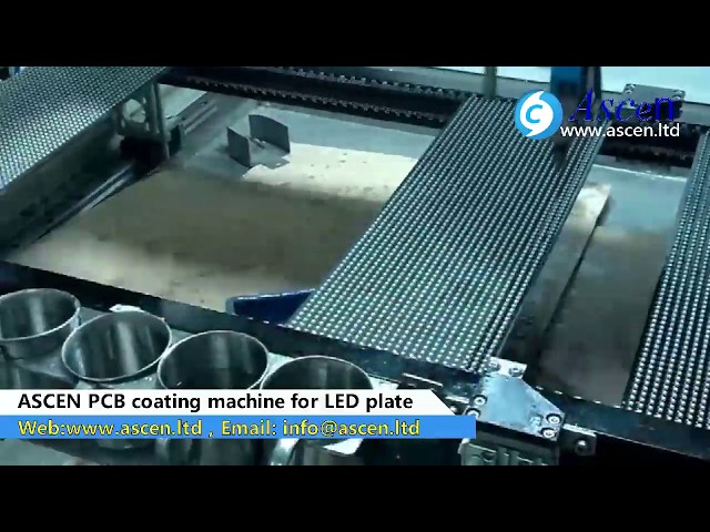
https://www.ascen.ltd/Products/conformal_coating_equipment//580.html PCB Conformal coating machine is used to paint conformal coating onto full LED panel to avoid PCB moisture,sault and static.It can be full panel conformal coating or selective coati

1200MM/1500MM Online SPI , Big Size Solder Paste Inspection Machine mail: sales@smtlinemachine.com whatapp/wechat:+8613537875415 Specification: 技术参数/Parameters 技术平台/Technology Platform super big size platform 适用
Events Calendar | Thu Mar 18 00:00:00 EDT 2021 - Thu Mar 18 00:00:00 EDT 2021 | ,
India Chapter Webinar: PCBA Process Qualifications
Career Center | San Jose, CA, California USA | Engineering,Production,Research and Development
Senior PCB Designer: Want to be part of an exciting pre-IPO enterprise B2B company working on the cutting edge of internet-of-things, artificial intelligence & agents, blockchain, and manufacturing technology? This well-funded venture-backed co
Career Center | Appleton, Wisconsin USA | Management,Purchasing
Manages controls and directs staff to achieve Materials profit and Loss objectives. Ensures the timely delivery of materials at the most economical cost, consistent with quality standards, affecting quality by assuring that suspicious material is ide
Career Center | Chennai, India | Sales/Marketing
Experience in sales of inter-connect, passive, active, and electro-mechanical components Product Engineering Role as handling BOM, ECO, ECN in the New product introduction of Philips LCD TV and Kulicke and Soffa wire bonding m/c Process and Quali
Career Center | sabarinathan95, India | Engineering,Maintenance,Quality Control
i am sabarinathan ap working in AVALON TECH PVT LTD at chennai as a QUALITY CONTROLLER and also have a knowledge in DEBUGGING and TESTING .i have 1 year experience in quality field.
A Study of PCB Insertion Loss Variation in Manufacturing Using a New Low Cost Metrology SMTnet Express June 27, 2012, Subscribers: 25268, Members: Companies: 8896, Users: 33235 A Study of PCB Insertion Loss Variation in Manufacturing Using a New
| https://www.eptac.com/faqs/ask-helena-leo/page/4
? Also, how do you avoid bubbles in the coating? Read More Vapor Phase Soldering to Immersion Tin Plated Pads QUESTION Question: I have a customer who seems to be having issues making acceptable solder connections using the vapor phase process
winsouce.jpg)
.gif)


