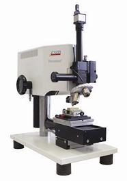
New Equipment | Test Equipment
The REVETEST® Scratch Testing instrument has become the industry standard for measuring hard-coated materials, with a typical coating thickness of several microns. Coatings may be organic or inorganic, covering Tribological, magnetic and decorative
Electronics Forum | Sat Apr 08 08:43:34 EDT 2000 | Dave F
Hi Gary: Generally: http://www.tmworld.com/db_prod/companiesbyproduct.cfm?PRODUCTCODENUMBER=201.0∏UCTNAME=Acoustic%20Emission%2FPIND%20Testers LR has a couple of used B&Ws for sale at: http://www.lre.com/test/searchresultx.asp But the coolest, l
Industry News | 2012-02-23 14:43:13.0
IPC has announced the winners of the Best U.S. and International Papers of IPC APEX EXPO® 2012. Selected through a ballot process by the event’s Technical Program Committee, the papers will be presented at IPC APEX EXPO, February 28–March 1, at the San Diego Convention Center.
Industry News | 2014-03-28 09:54:48.0
IPC – Association Connecting Electronics Industries® presented Committee Leadership, Distinguished Committee Service and Special Recognition Awards at IPC APEX EXPO® at Mandalay Bay Convention Center in Las Vegas.
Technical Library | 2015-08-13 15:52:40.0
Pad cratering has become more prevalent with the switch to lead free solders and lead free compatible laminates. This mainly is due to the use of higher reflow temperature, stiffer Pb-free solder alloys, and the more brittle Pb-free compatible laminates. However, pad cratering is difficult to detect by monitoring electric resistance since pad cratering initiates before an electrical failure occurs. Several methods have been developed to evaluate laminate materials' resistance to pad cratering. Pad-solder level tests include ball shear, ball pull and pin pull. The detailed methods for ball shear, ball pull, and pin pull testing are documented in an industry standard IPC-9708. Bansal, et al. proposed to use acoustic emission (AE) sensors to detect pad cratering during four-point bend test. Currently there is an industry-working group working on test guidelines for acoustic emission measurement during mechanical testing.
Technical Library | 2013-01-03 20:27:54.0
Electronics assemblies with large flip-chip BGA packages can be prone to either pad cratering or brittle intermetallic (IMC) failures under excessive PCB bending. Pad cratering cracks are not detected by electrical testing or non-destructive inspection methods, yet they pose a long term reliability risk since the cracks may propagate under subsequent loads to cause electrical failure. Since the initiation of pad cratering does not result in an instantaneous electrical signature, detecting the onset of this failure has been challenging. An acoustic emission methodology was recently developed by the authors to detect the onset of pad cratering. The instantaneous release of elastic energy associated with the initiation of an internal crack, i.e., Acoustic Emission (AE), can be monitored to accurately determine the onset of both pad cratering and brittle intermetallic (IMC) failures.

ACI Technologies Inc. (ACI) is a scientific research corporation dedicated to the advancement of electronics manufacturing processes and materials for The Department of Defense and industry. This video provides an overview of our commercial service
SMTnet Express, August 13, 2015, Subscribers: 23,186, Members: Companies: 14,558 , Users: 38,745 Pad Cratering Susceptibility Testing with Acoustic Emission Wong Boon San, Julie Silk; Agilent Technologies | Richard Nordstrom, Ph.D.; Acoustic
Investigation of Pad Cratering in Large Flip-Chip BGA using Acoustic Emission SMTnet Express January 3, 2013, Subscribers: 26072, Members: Companies: 9076, Users: 34113 Investigation of Pad Cratering in Large Flip-Chip BGA using Acoustic Emission
Surface Mount Technology Association (SMTA) | https://www.smta.org/iceet/workshops.cfm
The tools of FA and what they tell you with case studies Visual Inspection Metallurgical LSM XRAY imaging 2D 2.5D 3D Acoustic microscopy


