Industry Directory | Manufacturer
Adept Technology, Inc., founded in 1983, is America's largest manufacturer of industrial robots.

New Equipment | Industrial Automation
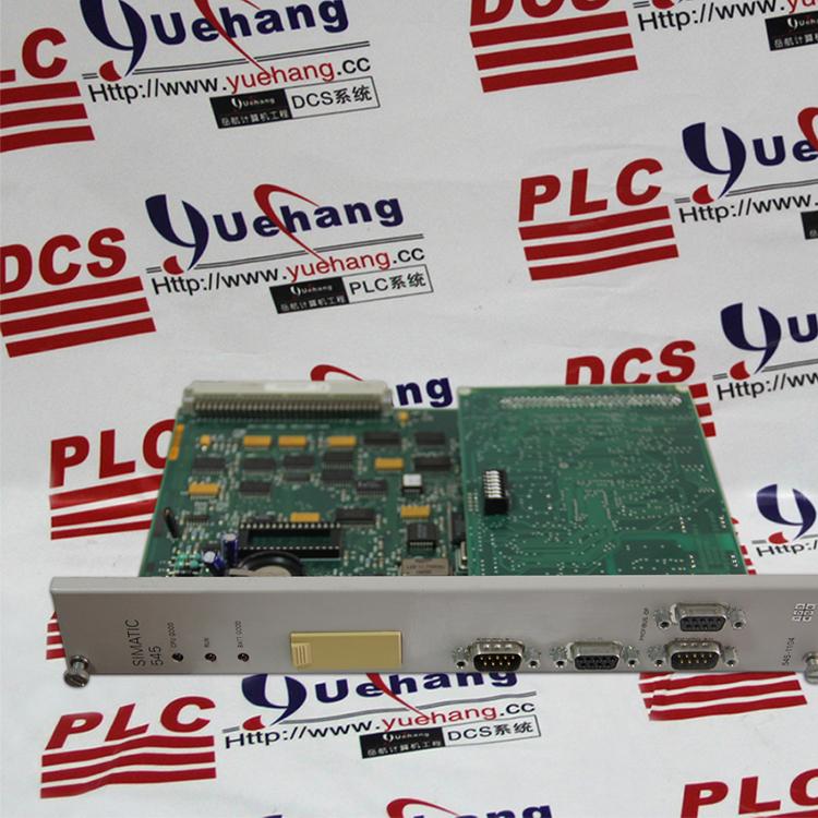
SANDY.[MAILTO:UNITY@MVME.CN] SANDY.[WHATSAPP/SKYPE/MOBILE:+8618020776786] SANDY.[QUOTE TO YOU WITHIN THE SHORTEST POSSIBLE TIME WITH OUR BEST PRICE] WARRANTY: UP TO 12 MONTHS SHIPPING: FAST DELIVERY IS AVAILABLE NEW+ORIGINAL+IN STOCK+ONE YE
New Equipment | Industrial Automation
SANDY.[MAILTO:UNITY@MVME.CN] SANDY.[WHATSAPP/SKYPE/MOBILE:+8618020776786] SANDY.[QUOTE TO YOU WITHIN THE SHORTEST POSSIBLE TIME WITH OUR BEST PRICE] WARRANTY: UP TO 12 MONTHS SHIPPING: FAST DELIVERY IS AVAILABLE NEW+ORIGINAL+IN STOCK+ONE YE
Electronics Forum | Wed Oct 04 10:12:16 EDT 2000 | pascal MATHIEU
go and see around the KUKA ,ADEPT and BOSCH brand they might be suitable for your project good luck bye bye
Electronics Forum | Thu Apr 13 17:56:01 EDT 2000 | David C.
Check out Robodyne Corp. We used them at Motorola, had some problems withthe Adept Software end of it, but the machine was capable.
Industry News | 2003-06-10 08:16:44.0
The following text describes the application of NWA Quality Analyst to quality control in the assembly of electronic components.
Surface Mount Technology Association (SMTA)
Technical Library | 2020-09-02 22:02:13.0
With the adoption of Wafer Level Packages (WLP) in the latest generation mobile handsets, the Printed Circuit Board (PCB) industry has also seen the initial steps of High Density Interconnect (HDI) products migrating away from the current subtractive processes towards a more technically adept technique, based on an advanced modified Semi Additive Process (amSAP). This pattern plate process enables line and space features in the region of 20um to be produced, in combination with fully filled, laser formed microvias. However, in order to achieve these process demands, a step change in the performance of the chemical processes used for metallization of the microvia is essential. In the electroless Copper process, the critical activator step often risks cross contamination by the preceding chemistries. Such events can lead to uncontrolled buildup of Palladium rich residues on the panel surface, which can subsequently inhibit etching and lead to short circuits between the final traces. In addition, with more demands being placed on the microvia, the need for a high uniformity Copper layer has become paramount, unfortunately, as microvia shape is often far from ideal, the deposition or "throw" characteristics of the Copper bath itself are also of critical importance. This "high throwing power" is influential elsewhere in the amSAP technique, as it leads to a thinner surface Copper layer, which aids the etching process and enables the ultra-fine features being demanded by today's high end PCB applications. This paper discusses the performance of an electroless Copper plating process that has been developed to satisfy the needs of challenging amSAP applications. Through the use of a radical predip chemistry, the formation, build up and deposition of uncontrolled Pd residues arising from activator contamination has been virtually eradicated. With the adoption of a high throwing power Copper bath, sub 30um features are enabled and microvia coverage is shown to be greatly improved, even in complex via shapes which would otherwise suffer from uneven coverage and risk premature failure in service. Through a mixture of development and production data, this paper aims to highlight the benefits and robust performance of the new electroless Copper process for amSAP applications
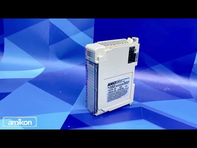
>>CONTACT MAC NOW Email: at@mooreplc.com Mobile: +8618020714662(Whatsapp) Skype: +8618020714662 >>>CONTACT MAC NOW ✦ Quick Details ✦ Place of Origin: USA Brand Name: ADEPT Certification: CO.CQ
>>CONTACT MAC NOW Email: at@mooreplc.com Mobile: +8618020714662(Whatsapp) Skype: +8618020714662 >>>CONTACT MAC NOW ✦ Quick Details ✦ Brand:Other Item NO.:ADEPT AWCII 040 Order(MOQ):1 Payment:T/T Color:Brand New
Career Center | Woburn, Massachusetts USA | Sales/Marketing
We seek an ambitious, technically adept professional to develop and maintain business relationships with OEM�s and Contract Manufacturers. As a Professional Sales Engineer, you will represent PCC with potential & existing customers within a defin
Career Center | Gaithersburg, Maryland USA | Production
Acquire materials from inventory and verify quantities against Work Order Documentation. Load part feeders and up SMT equipment according to Up Documentation. Operate SMT equipment safely per Manufacturer's Operating Manual and in-house SMT guideli
Career Center | , | Maintenance
Specialized in Siemens equipment, and OmniExcel 7, MPM Ap25, Momentum.
Career Center | Kitchener, Ontario Canada | Engineering,Maintenance,Technical Support
Knowledgeable in Design of Experiments (DOE), Design for Manufacturability (DFM), Statistical Process Control (SPC), Failure Mode & Effects Analysis (FMEA) and Root Cause Analysis that drives continuous improvement in package reliability. A recogniz
Imagineering, Inc. | https://www.pcbnet.com/blog/advantages-and-disadvantages-of-polyimide-pcbs/
. It has a long life, is less brittle than rigid printed circuit board materials, and is resistant to heat. Advantages of Polyimide PCBs Although they may be more expensive than typical FR-4 materials, polyimide material is adept at conforming to unusual environments that would test the limits of more


winsouce.jpg)