Industry Directory | Consultant / Service Provider / Manufacturer
Established in 1990 and accumulated years of experiences in providing laser-plotting service to sample and mass production, Plotech has become a high-end PCB leader with all High Mix & High Volume facilities in South East Asia.
Industry Directory | Manufacturer
A printed circuit board manufacturer producing high quality prototype printed circuit boards.
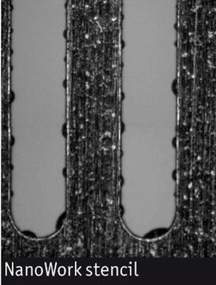
New Equipment | Solder Paste Stencils
Laser cut stainless steel stencil with nano coating from LaserJob. The patented NanoWork - stencil from LaserJob is based on a laser cut SMD stencil. Since 2007 LaserJob coates SMD - stencils and step stencils in an in-house process. The NanoWork co

Innovative Materials, Superior Performance. Our printed circuit board and semiconductor packaging materials provide superior thermal and mechanical performance, a fact we’ve prided ourselves on for over 45 years. All our materials are RoHS complian
Electronics Forum | Tue May 22 20:27:34 EDT 2007 | davef
What are the area and aspect ratio of the apertures that clog? When you print, you should be able to fit at least 4 of the mean sized solder sphere across the width or diameter of your smallest apertures.
Electronics Forum | Wed Apr 14 14:51:10 EDT 2010 | jgalarza
After checking some of our stencil data for the correct aspect ratio I found that a few are wrong. I would like to change them from 5mil thk to 4mil thk but do not know how much paste volume I need to keep. We are using 0201,0402, and BGA with 0.80 p
Industry News | 2018-10-18 08:59:34.0
PRINCIPLE OF SURFACE MOUNT PROCESS(SMT PROCESS)
Industry News | 2018-12-08 03:29:29.0
SMT Dictionary – Surface Mount Technology Acronym and Abbreviation
Technical Library | 2013-03-07 18:25:36.0
The market for high-layer-count printed circuit boards (PCB) containing blind and buried vias was once relatively small, and focused on specialized applications in the military and high end computing. The demand for these types of PCBs today is being driven by an increasing number of commercial applications in the telecommunications and semiconductor test market segments. These applications typically require high-aspect-ratio plated-through-holes (PTHs) and blind and buried vias in order to meet the applications interconnect density requirements. Blind and buried vias and high aspect ratio PTHs continue to present manufacturing challenges and frequently are the limiting features to achieving high fabrication yield... First published in the 2012 IPC APEX EXPO technical conference proceedings
Technical Library | 2018-06-13 11:42:00.0
The art of screen printing solder paste for the surface mount community has been discussed and presented for several decades. However, the impending introduction of passive Metric 0201 devices has reopened the need to re-evaluate the printing process and the influence of stencil architecture. The impact of introducing apertures with architectural dimensions’ sub 150um whilst accommodating the requirements of the standard suite of surface mount connectors, passives and integrated circuits will require a greater knowledge of the solder paste printing process.The dilemma of including the next generation of surface mount devices into this new heterogeneous environment will create area ratio challenges that fall below todays 0.5 threshold. Within this paper the issues of printing challenging area ratio and their associated aspect ratio will be investigated. The findings will be considered against the next generation of surface mount devices.
Career Center | Houston, Texas USA | Engineering,Management,Production
SMT Manufacturing Engineer – 2nd Shift Hunting Innova is a Houston based company serving industrial, energy, medical, defense and aerospace segments of the Electronic Manufacturing Services (EMS) Industry since 1989. Hunting Innova is located in N
Career Center | Bangalore, India | Engineering,Maintenance,Production,Technical Support
SMT Stencil designing & Knowledge of full SMT process software known CAD/CAM -circuit CAM Pro 7.3,GC Power station, GCCAM Edit,Auto CAD, Fault finding of Electronic Boards & Servicing electronic machines.
SMTnet Express, June 14, 2018, Subscribers: 31,125, Companies: 10,958, Users: 24,820 Unlocking The Mystery of Aperture Architecture for Fine Line Printing Clive Ashmore; ASM Assembly Systems The art of screen printing solder paste for the surface
SMTnet Express, September 28, 2017, Subscribers: 30,862, Companies: 10,741, Users: 23,873 An Investigation into the Use of Nano-Coated Stencils to Improve Solder Paste Printing with Small Stencil Aperture Area Ratios Jasbir Bath, Tony Lentz, Greg
Imagineering, Inc. | https://www.pcbnet.com/blog/the-ever-changing-world-of-pcbs-in-aerospace-applications/
. Therefore, PCBs in the industry are designed with high aspect ratios. The ratio describes the relationship between the dimensions of the board and the via circuit
| http://etasmt.com/cc?ID=te_news_industry,26765&url=_print
. The aperture size is also relevant since the relation (aspect ratio) between this and the material thickness will determine if the release of solder paste is optimal


