Industry Directory | Manufacturer
Micralyne offers a patented process for electroplating AuSn solder alloy, at compositions from 10 to 40 Sn (wt%), in patterned or unpatterned shapes onto metallized substrates at virtually any thickness.
Industry Directory | Manufacturer
We are manufacturer of key products for semiconductor back end process and interconnect materials. Our main products:solder balls, Bonding wire (Au, Ag, Cu, Pd-Cu),sputtering target & EVM materials.

Automobile mechanical parts coating , cell phone buttons point glue , mobile phone battery packaging,laptop battery packaging , the coil point glue , PCB bonding / sealing , IC bonding / sealing , horn external punctuate glue , PDA sealing , LCD
New Equipment | Solder Materials
AuSn solder electroplating is a key technology developed by Micralyne to lower your production costs and give you a better MEMS product. This state-of-the-art, patented process for electroplating AuSn solder alloy is a giant step forward in electropl
Electronics Forum | Mon Sep 20 11:21:48 EDT 2010 | tony1
I have this NiPdAu small QFN packge sizes less than 2x2. I tried to do solderability Dip And Look test and there's always some units no wet on either ground pad and small I/O. Can someone help to explain why is this so difficult to set on this surfac
Electronics Forum | Wed Sep 22 15:33:54 EDT 2010 | davef
Comments are: * First, no one is looking at your posting. You need to post in the 'SMTnet Production Forum' [top of the page]. This 'SMTnet Site Support Forum' is for whiners that want to complain to Neil about problems in logging-in, font that's to
Industry News | 2003-03-11 08:45:00.0
CAMtastic DXP is the latest version of Altium's complete CAM verification and editing system that bridges the gap between PCB design and manufacturing and facilitates communication between board designers, fabrication engineers, and their clients.
Industry News | 2013-08-01 13:16:42.0
The SMTA announced that the Lead-Free Soldering Technology Symposium will be held on October 17, 2013 as a focused symposium at SMTA International in Fort Worth, TX.
Parts & Supplies | SMT Equipment
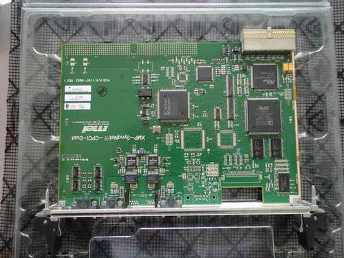
XMP card of KE2050 Professional maintenance JUKI SMT various circuit boards: JUKI CPU motherboard, SUB-CPU board, laser control board, servo drive card, X / Y / Z / Q-axis drive, 24V power supply card, head boards, image control card, I / O board
Parts & Supplies | SMD Placement Machines
PANASERT / UNIVERSAL / DYNAPERT PARTS FOR SALE N434UQ04041 Tube BLKE01252 FUSE 5A 40833025 FUSE 1.5A 42453904 FUSE 5A 42453907 FUSE 1A 46347803 Relay 40525301 SHOCK ABSORBER KXF0DSSAA00 46849802 SENSOR 46347803 RELAY 47323702 PROX SWITCH PNP N
Technical Library | 2013-08-29 19:52:43.0
Au over Ni on Cu is a widely used printed circuit board (PCB) surface finish, under bump metallization (UBM), and component lead metallization. It is generally accepted that less than 3 wt.% Au in Sn-Pb solder joints inhibits formation of detrimental intermetallic compounds (IMC). However, the critical limit for Au content in Pb-free solder joints is not well established. Three surface-mount package platforms, one with a matte Sn surface finish and the others with Ni/Au finish, were soldered to Ni/Au-finished PCB using Sn-3.0Ag 0.5Cu (SAC305) solder, in a realistic manufacturing setting. The assembled boards were divided into three groups: one without any thermal treatment, one subjected to isothermal aging at 125°C for 30 days, and the third group aged at 125°C for 56 days...
Technical Library | 2017-02-28 12:39:50.0
During the last 5 years mobile phones and other portable consumer electronics have been extremely popular and spread all over the world in different climate zones in very high volumes. At the same time the mobile phone terminal for many people has become a necessity that is brought with them in any activity they practice. These changes in user behavior have heavily changed the impact on handheld terminals from moisture, sweat, corrosive atmospheres and mechanical drop. As a result of this the requirement to solder joint reliability, corrosion stability and wear resistance are heavily increasing to keep a high reliability of the terminal.Immersion Ni/Au has been the overall dominant surface finish on Printed Wiring Boards (PWB's) for the last 10 years, but a paradigm shift to avoid use of this thin and porous surface finish is ongoing nowadays because it can’t address these challenges in a satisfactory way.In today's handheld terminals, Organic Solder Preservative (OSP) has replaced Immersion Ni/Au on solder pads. Carbon surface finish for Key- and spring contact-pads, combined with the right concept design can make use of Immersion Ni/Au unnecessary in the near future. The result will be higher reliability with less expensive and simpler processes.This paper will discuss the various considerations for choice of surface finish and results from the feasibility studies performed.

1200MM/1500MM Online SPI , Big Size Solder Paste Inspection Machine mail: sales@smtlinemachine.com whatapp/wechat:+8613537875415 Specification: 技术参数/Parameters 技术平台/Technology Platform super big size platform 适用
Inline 3D SPI, Standard Automatic solder paste inspection system As one of the strongest SMT 3D SPI Manufacuturer in China, we provide you all the different models of online solder paste inspection machine,we have variety of size and models of the
Career Center | St. Léonard, Quebec Canada | Production
Joignez-vous à Schneider Electric et propulsez votre carrière! Découvrez l’occasion rêvée de vous joindre à une entreprise internationale, dynamique et responsable qui encourage le développement de tous ses employés à travers le monde. Chaque jour,
SMTnet Express August 29, 2013, Subscribers: 26233, Members: Companies: 13474, Users: 35110 Effect of Gold Content on the Microstructural Evolution of SAC305 Solder Joints Under Isothermal Aging by Mike Powers, Jianbiao Pan, Julie Silk, Patrick
The Morphology Evolution and Voiding of Solder Joints on QFN Central Pads with a Ni/Au Finish SMTnet Express October 19, 2012, Subscribers: 25598, Members: Companies: 9011, Users: 33828 The Morphology Evolution and Voiding of Solder Joints on QFN
| https://www.eptac.com/wp-content/uploads/2007/10/webinar_eptac_10_17_07.pdf
Heller Industries Inc. | https://hellerindustries.com/wp-content/uploads/2022/06/Optimizing-Reflowed-Solder-TIM-sTIMs-Processes-for-Emerging-Heterogeneous.pdf
to be joined using sTIM are usually gold, with the silicon backside typically being PVD-deposited Ti/NiV/Au (80-200nm Au), and copper heatspreader/lids plated with Ni/Au (usually with 0.3-0.8um Au). Except for the inevitable presence of a film of


