Industry Directory | Manufacturer
professional manufacturer of pcb
Industry Directory | Manufacturer
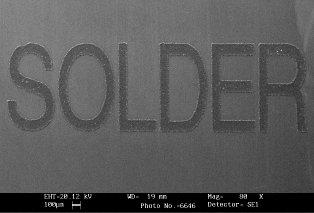
Micralyne offers a patented process for electroplating AuSn solder alloy, at compositions from 10 to 40 Sn (wt%), in patterned or unpatterned shapes onto metallized substrates at virtually any thickness.
New Equipment | Solder Materials
AuSn solder electroplating is a key technology developed by Micralyne to lower your production costs and give you a better MEMS product. This state-of-the-art, patented process for electroplating AuSn solder alloy is a giant step forward in electropl
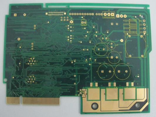
Layer: 10L Base Material:FR-4 tg180(ITEQ) Board Thickness: 1.6mm Final copper: 35um Surface Finish:Immersion Gold/Au:2u” min. Gold fingers/Au:30u” Solder mask: Green Profile: Routing E-test: 100% Fixture Quality report: Solderability test, Fi
Electronics Forum | Thu Oct 02 17:54:46 EDT 2003 | davef
Yes, Russ IPC-6012A w A#1 - Qualification & Performance For Rigid Printed Boards talks to solder mask requirements in 3.8. One interpretation of what it says: * Solder resist [solder mask] must meet the qualification / conformance requirements of S
Electronics Forum | Mon Feb 19 18:57:49 EST 2001 | davef
Expanding on the limit of the portion of gold acceptable in a solder connection [mentioned in an earlier post]: The embrittlement culprit, AuSn4, is 29 weight percent gold. So even if one had 100% tin as the solder alloy and 10% gold were dissolved
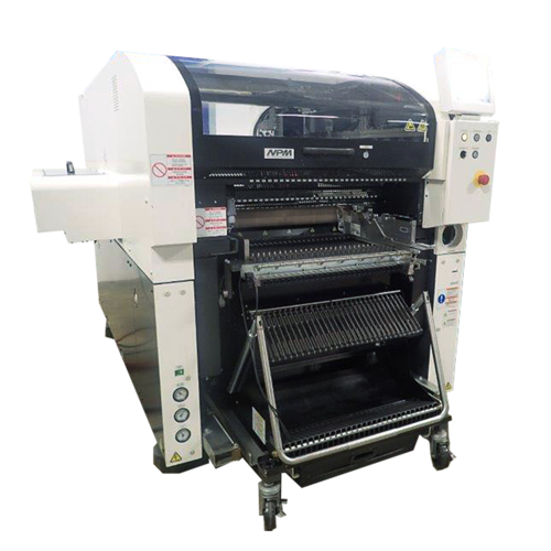
Used SMT Equipment | Pick and Place/Feeders
Panasonic Modular Chip Mounter NPM-W2 NM-EJM7D Feature▶Model NM-EJM7D with 3,8,12,and 16 Light-weight Placements heads provide production flexibility.▶Max Speed:77,000 CPH.▶Support PCB size Max:750*550MM.▶Support up to 120 8MM tap feeder slots.
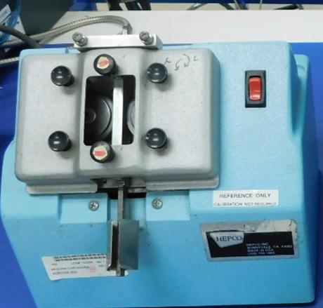
Used SMT Equipment | General Purpose Test & Measurement
Hepco 7900-LF3 DIP Lead FormerSN: 1703 General specs:Series 7900 Convertible DIP Lead FormersAutomatically Adjusts for Body Thickness Variations.One Machine for .300", .400" and .600" DIPS Fast, Simple Conversion - Under 2 Minutes.Fixed Tooling Means
Industry News | 2003-06-18 08:04:27.0
Recently purchased and installed a new DP-1500-2X Dual-Sided Photoimageable Ink Coater from Circuit Automation
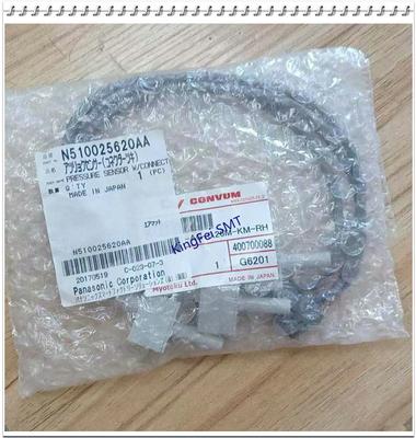
Parts & Supplies | Pick and Place/Feeders
N210095370AA COVER 0 KXFB0AU3A00 POST 0 KXF0E0NMA00 PLUG CP-30-HP-1 N210046856AA BRACKET 0 N510017083AA SPACER BSF-430E N510018125AA SCREW Cross recessed Countersunk head machine screw M2.5X8-4.8 A2J (Trivalen N210028733AA PLATE 0 KXFX064BA00
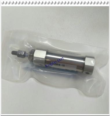
Parts & Supplies | Pick and Place/Feeders
N510017368AA BOLT Hexagon socket head cap screw M4X45-10.9 A2J (Trivalent) N510004786AA POST ETKRFT-25-250-1 N610018132AA COVER 0 MTNP000804AA JOINT KQ2W08-U01A N510020431AB CASE Mount Position Teach Jig Case N510018857AA BOLT Hexagon head bolt
Technical Library | 2023-08-04 15:27:30.0
A designed experiment evaluated the influence of several variables on appearance and strength of Pb-free solder joints. Components, with leads finished with nickel-palladium-gold (NiPdAu), were used from Texas Instruments (TI) and two other integrated circuit suppliers. Pb-free solder paste used was tin-silver-copper (SnAgCu) alloy. Variables were printed wiring board (PWB) pad size/stencil aperture (the pad finish was consistent; electrolysis Ni/immersion Au), reflow atmosphere, reflow temperature, Pd thickness in the NiPdAu finish, and thermal aging. Height of solder wetting to component lead sides was measured for both ceramic plate and PWB soldering. A third response was solder joint strength; a "lead pull" test determined the maximum force needed to pull the component lead from the PWB. This paper presents a statistical analysis of the designed experiment. Reflow atmosphere and pad size/stencil aperture have the greatest contribution to the height of lead side wetting. Reflow temperature, palladium thickness, and preconditioning had very little impact on side-wetting height. For lead pull, variance in the data was relatively small and the factors tested had little impact.
Technical Library | 2014-11-06 16:43:24.0
This paper summarizes the results of recent investigations to examine the effect of electroless nickel process variations with respect to Pb-free (Sn-3.0Ag-0.5Cu) solder connections. These investigations included both ENIG and NiPd as surface finishes intended for second level interconnects in BGA applications. Process variations that are suspected to weaken solder joint reliability, including treatment time and pH, were used to achieve differences in nickel layer composition. Immersion gold deposits were also varied, but were directly dependent upon the plated nickel characteristics. In contrast to gold, different electroless palladium thicknesses were independently achieved by treatment time adjustments.

Flux spray coating on a PCB with uniformal thickness down to 5 microns, with clear edge definition and minimal overspray. Can coat large or shoot dots with the same jet.
UV Laser PCB Depaneling System, Dual Table for High Volume Laser Depaneling Purpose: The processing and application objects are PCB, FPC soft and hard plate and related material cutting, cover opening and other operations. Efficient integration
Training Courses | | | PCB Design Courses
The PCB design courses teach students the process, techniques and tools needed to design layout of printed circuit boards.
The Morphology Evolution and Voiding of Solder Joints on QFN Central Pads with a Ni/Au Finish SMTnet Express October 19, 2012, Subscribers: 25598, Members: Companies: 9011, Users: 33828 The Morphology Evolution and Voiding of Solder Joints on QFN
Imagineering, Inc. | https://www.pcbnet.com/capabilities/assembly/tolerances/
. They provide enough variation for us to assemble your board – and for it to work properly in your application. Supported PC Board Specs: Min size: 1.967 in. X 1.967 in. Max size: 19.67 in. X 19.67 in. Min thickness: 4 mil Max thickness: 240 mil Layer Count: Up to 24 Finishes: HASL, ENIG, Silver


