
Industry Directory | Training Provider / Manufacturer's Representative / Equipment Dealer / Broker / Auctions / Consultant / Service Provider
Products, services, training & consulting for the assembly, rework & repair of electronic assemblies. BGA process experts. Manufacturers Rep, Distributor & Service Provider for Seamark/Zhuomao and Shuttle Star BGA Rework Stations.
Industry Directory | Manufacturer
Thermally Managed ( up to 1000 W /m K thermal transfer rate ), CTE controlled, Very Rigid, Light Weight STABLCOR PCB / Substrate Technology
New Equipment | Assembly Services
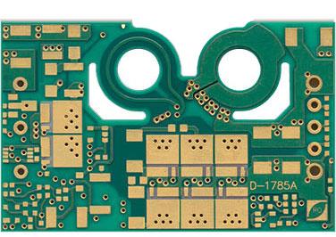
Heavy Copper Printed Circuits supplier Saturn Electronics Corp., bare printed circuit board manufacturer, was one of North America's largest users of heavy copper PCB laminate, which we used in the bare PCB manufacturing of Power Distribution Boards
New Equipment | Assembly Services
1,012 (normal) Electric strength: >1.3kV/mm Thermal stress: 288°C, 20 seconds Testing voltage: 50 to 300V Packing: vacuum packing for PCB, and good condition outer boxes
Electronics Forum | Mon Dec 16 10:05:29 EST 2002 | Grant Petty
Hi, Thanks for the info. We are reflowing the boards, but just barely. Sometimes we get the QFP in the middle of the copper area not reflowing, and it's pain. The joints are dry, and I am not sure if it's caused by lack of heat, or the flux going ba
Electronics Forum | Wed Jun 27 21:05:48 EDT 2001 | davef
BGA Cycle 1: solder ball attach. BGA Cycle 2: BGA attach to board. BGA Cycle 3: BGA removal from board. BGA Cycle 4: BGA pad dress. BGA Cycle 5: BGA ball replacement. BGA Cycle 6: BGA re-attach to board. Board Cycle 1: BGA attach to board. Boar

Used SMT Equipment | Soldering Equipment/Fluxes
Versaflow Selective soldering Selective Soldering Process Advantages: Better, Faster, Cleaner & Cheaper! . consistent LF solder joint quality & significant reduction of DPM . No re-melting of top side SMD components, as with wave soldering . PCB
Industry News | 2019-03-10 20:30:11.0
The proliferation of tighter microvia densities and signal integrity requirements in printed boards within the electronics industry has revealed reliability concerns with microvia structures in high performance products. A number of IPC OEM member companies have approached IPC with examples of microvia failures in high-profile hardware that were not observed until after bare printed board fabrication, inspection and acceptance, including:
Industry News | 2018-04-22 19:12:45.0
SMTA Europe announces Session 7 Technical Program on High Temperature PCB Materials and Fabrication at the “Electronics in Harsh Environments Conference” to be held in Amsterdam, Netherlands, on April 25th, 2018.
.jpg)
Parts & Supplies | Pick and Place/Feeders
Supply&repair juki spare parts at l lower price: JUKI 710(720) CARRY UNIT E86127150B0 JUKI 710(720) CPU CARD E8601715AA0 JUKI 730(740) CARRY BOARD E86067210A0 JUKI 730(740) DC SERVO DRIVER E86037210A0 JUKI 750(760) AC SERVO CARD E86027210A0
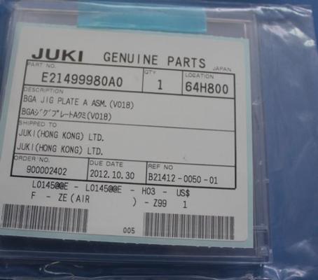
Parts & Supplies | Assembly Accessories
JUKI NGA JIP PLATE A ASM E21499980A0 We are Supply SMT Pick and Place Equipment spare parts(Smt nozzle, Smt Cylinder, Smt Valve, Smt Sensor, Smt Feeder, Smt CPU Board, Smt Laser, Smt driver, Smt ejector……) for Yamaha, JUKI, FUJI ,Panasonic, Samsun
Technical Library | 2021-09-02 08:17:07.0
We are a professional manufacturer of PCB depaneling machines, which is workable for all boards, including flex and regid boards, v-scored boards and routed boards. Laser pcb depaneling is non-contact way without mechanical stress,this solution is good for modern precision PCB depaneling. It has below advantages: 1. No dust The production environment of the circuit board industry is carried out in the dust-free workshop. The traditional pcb depaneling equipment, such as blade moving type machine, will inevitably produce residues and micro powder, which will pollute the 10000 and 1000 class dust-free workshops and affect the conductivity of products. The UV laser PCB cutting machine is a vaporization processing process, which will not produce dust and is conducive to the conductivity of the product. 2. High cutting precision The processing gap of high-precision traditional processing equipment can not reach the gap width of less than 100 microns, which will cause certain damage to the lines on the edge or PCBA circuit board containing components. The focus spot of the laser cutting machine is small, and the ultraviolet cold processing mode has little thermal impact on the edge of the circuit board. The cutting position accuracy is less than 50 microns, and the cutting size accuracy is less than 30 microns, which will not affect the edge of the circuit board, and the precision is high. 3. No stress Traditional processing methods generally have V-grooves, which will cause certain damage to the board in the manufacturing process. The UV laser PCB cutting machine can directly cut the bare board without making V-grooves. In addition, the traditional processing methods directly use tools to act on the circuit board, especially the stamping method has a great impact on the circuit board, which is easy to cause board deformation. The laser cutting machine is a non-contact processing mode, which acts on the surface of the material through the high-energy beam, which will not cause the influence of stress and the deformation and damage of the circuit board. 4. For special-shaped cutting, it is easy to automate The UV laser PCB cutting machine can cut for any shape without replacing any props and fixtures, and without steel mesh. The same equipment can meet special-shaped and straight-line cutting, which is easy to realize assembly line automatic production and high flexibility. It is easy to improve production efficiency and save production process and production cycle. In particular, it can quickly and efficiently meet the needs of rapid proofing, directly import the drawing, and then locate the cutting. 5. High compatibility The UV laser PCB cutting machine can process the materials around the circuit board, such as PCB, FPC, covering film, pet, reinforcing board, IC, ultra-thin metal cutting, etc. it has strong practicability, is compatible with the processing of a variety of materials, is easy to operate, can be imported into the drawing, does not need to adjust any mechanical parts, and is easy to operate and maintain. 6. Good cutting edge effect The cutting edge is smooth and neat without burr. It can be processed and formed directly according to the size of the drawing, which is conducive to improving the yield of the product. It can be directly installed into the subsequent process without further processing. For more details about UV laser depaneling, please feel free to contact us. www.pcbdepanelingrouter.com
Technical Library | 2011-10-20 22:03:30.0
Results of FEM modelling of thermal stress analysis in printed circuit boards are given in the article. It is shown that thermal stress alone is not solely caused by differences in coefficients of thermal expansion of individual layers. The emergence of thermal stress is subject to both the layered structure of the wall and given boundary conditions, as well as the existence of a temperature gradient in the direction normal to the surface of the wall. A practical application focuses on the issue of recycling of PCB with the effort to achieve separation of layers due to thermal stress. Role modelling of thermal stress in this area lies in predicting the possibility of separation, depending on the type of thermal stress and material parameters.

ACI Technologies Inc. (ACI) is a scientific research corporation dedicated to the advancement of electronics manufacturing processes and materials for The Department of Defense and industry. This video provides an overview of our commercial service
UV Laser PCB Depaneling System, Dual Table for High Volume Laser Depaneling Purpose: The processing and application objects are PCB, FPC soft and hard plate and related material cutting, cover opening and other operations. Efficient integration
Career Center | Murphy, North Carolina USA | Engineering
We are seeking a qualified and experienced senior design engineer to join our team. The best candidate will use both mechanical and electrical engineering skills to design innovative power supplies that are highly efficient, rugged, and have high rel
Career Center | Thanjavur, India | Production,Quality Control,Technical Support
work in one year and above Quality engineer in sanmina,current work in SMT Technical engineer in coimbatore
Career Center | tulsa, Oklahoma | Engineering
Printed Circuit Assembly Process Engineer. Seeking a position in a high-technology operation, utilizing my background supporting a progressive and growth-oriented organization. Offering the technical experience, expertise, and skills gained during th
Modelling of Thermal Stresses in Printed Circuit Boards Modelling of Thermal Stresses in Printed Circuit Boards Results of FEM modelling of thermal stress analysis in printed circuit boards are given in the article. It is shown that thermal
Embedded Thermoelectric Cooling Article Embedded Thermoelectric Cooling Thin film thermoelectric devices offer a fundamentally new operating regime for integrated, active cooling solutions and localized thermal management, yet the assembly
Imagineering, Inc. | https://www.pcbnet.com/blog/the-importance-of-thermal-management-in-pcb-manufacturing/
The Importance of Thermal Management in PCB Manufacturing | Imagineering, Inc. Skip to main content Resources Support Contact Us FAQs Live Chat My Account 847-806-0003 Menu PCB Capabilities Fabrication Technology Roadmap Materials Available HDI Tolerances Certifications
Heller 公司 | http://hellerindustries.com.cn/Vacuum-Void-Reduction-Reflow.pdf
thermal expansion (CTE) mismatch between the package and the PCB [20, 21]. The CTE of the PCB was measured using a thermomechanical analyzer (TMA) and the composite coefficients of thermal expansion of the 192CABGA and 84CTBGA packages were measured using
Products, services, training & consulting for the assembly, rework & repair of electronic assemblies. BGA process experts. Manufacturers Rep, Distributor & Service Provider for Seamark/Zhuomao and Shuttle Star BGA Rework Stations.
Training Provider / Manufacturer's Representative / Equipment Dealer / Broker / Auctions / Consultant / Service Provider
1750 Mitchell Ave.
Oroville, CA USA
Phone: (888) 406-2830


