Industry Directory | Manufacturer
NM Laser offers quality laser beam shutters across the US, UK, and major European and Asian markets.
Industry Directory | Manufacturer
Dedicated & Flexible Custom Assembly for Industry
Our Preco FlexPro CNC laser cutting system provides the speed of galvanometer processing with all the versatility of an XY motion system. Orion has the capability to cut detailed parts more precisely, and with shorter lead-times than conventional too

The FKN Systek K4000 motorized linear blade depanelizer is designed for high volume singulation of scored and skip scored Printed Circuit Boards. No programming necessary. (Switch select operating mode and speed) Singulate panels with components
Electronics Forum | Mon Jul 21 14:29:25 EDT 2003 | Claude_Couture
What's a Panasonic Soft Beam? What does it do?
Electronics Forum | Thu Oct 28 14:10:50 EDT 2010 | jj12345
- Can anyone please tell me how to change the teaching to the vision camera instead of the beam sensor. In the machine configurations i have - Beam Sensor : Yes (yes/no) and Teaching Camera : Yes (yes/no), so it should default to the teaching camera
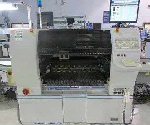
Used SMT Equipment | Pick and Place/Feeders
OS: Windows XP SW: 8.5.5.1 Lightning Feature Cameras: OTHC (Narrow fov) beam 1 firewire 1394 .55 per pixel. OTHC (Narrow fov) beam 2 firewire 1394 .55 per pixel. Pecs: pec beam1 firewire 1394 1.0 mil per pixel. pec beam 2 firewire
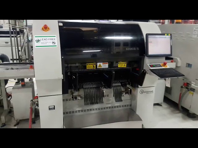
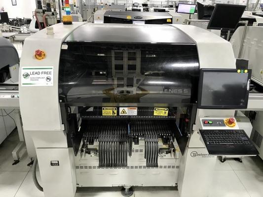
Used SMT Equipment | Pick and Place/Feeders
Serial: 10101112 Windows XP SW: 8.5.5.1 Lightning Feature Cameras: OTHC (Narrow fov) beam 1 firewire 1394 .55 per pixel. OTHC (Narrow fov) beam 2 firewire 1394 .55 per pixel. Pecs: pec beam1 firewire 1394 1.0 mil per pixel
Industry News | 2003-06-04 09:19:23.0
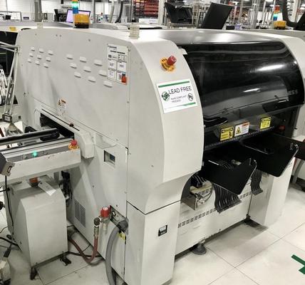
With increasing demand for fine pitch placements and a growing amount of fast turnaround high-tech low-volume prototype work, Speedboard has invested in additional SMT/BGA placement/rework equipment.
Industry News | 2017-07-18 13:16:28.0
Depanelizing skip routed PCB panels up to 48" long is made simple and easy with FKN Systek’s K4000 PCB singulator. Just place the bottom scoreline of the PCB onto the linear blade and step on a guarded foot switch to bring the circular blade across the top scoreline for clean separation of the PCB panels. Right and left blade guards assure operator safety. The front and back support and take up table are height adjustable.

Technical Library | 2021-09-02 08:17:07.0
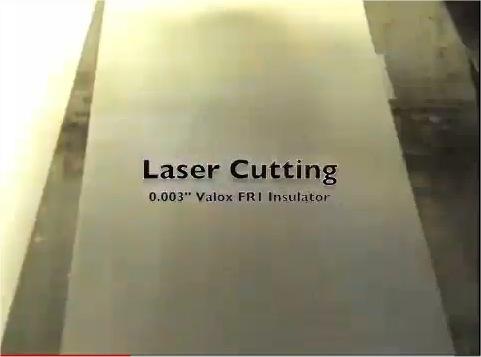
We are a professional manufacturer of PCB depaneling machines, which is workable for all boards, including flex and regid boards, v-scored boards and routed boards. Laser pcb depaneling is non-contact way without mechanical stress,this solution is good for modern precision PCB depaneling. It has below advantages: 1. No dust The production environment of the circuit board industry is carried out in the dust-free workshop. The traditional pcb depaneling equipment, such as blade moving type machine, will inevitably produce residues and micro powder, which will pollute the 10000 and 1000 class dust-free workshops and affect the conductivity of products. The UV laser PCB cutting machine is a vaporization processing process, which will not produce dust and is conducive to the conductivity of the product. 2. High cutting precision The processing gap of high-precision traditional processing equipment can not reach the gap width of less than 100 microns, which will cause certain damage to the lines on the edge or PCBA circuit board containing components. The focus spot of the laser cutting machine is small, and the ultraviolet cold processing mode has little thermal impact on the edge of the circuit board. The cutting position accuracy is less than 50 microns, and the cutting size accuracy is less than 30 microns, which will not affect the edge of the circuit board, and the precision is high. 3. No stress Traditional processing methods generally have V-grooves, which will cause certain damage to the board in the manufacturing process. The UV laser PCB cutting machine can directly cut the bare board without making V-grooves. In addition, the traditional processing methods directly use tools to act on the circuit board, especially the stamping method has a great impact on the circuit board, which is easy to cause board deformation. The laser cutting machine is a non-contact processing mode, which acts on the surface of the material through the high-energy beam, which will not cause the influence of stress and the deformation and damage of the circuit board. 4. For special-shaped cutting, it is easy to automate The UV laser PCB cutting machine can cut for any shape without replacing any props and fixtures, and without steel mesh. The same equipment can meet special-shaped and straight-line cutting, which is easy to realize assembly line automatic production and high flexibility. It is easy to improve production efficiency and save production process and production cycle. In particular, it can quickly and efficiently meet the needs of rapid proofing, directly import the drawing, and then locate the cutting. 5. High compatibility The UV laser PCB cutting machine can process the materials around the circuit board, such as PCB, FPC, covering film, pet, reinforcing board, IC, ultra-thin metal cutting, etc. it has strong practicability, is compatible with the processing of a variety of materials, is easy to operate, can be imported into the drawing, does not need to adjust any mechanical parts, and is easy to operate and maintain. 6. Good cutting edge effect The cutting edge is smooth and neat without burr. It can be processed and formed directly according to the size of the drawing, which is conducive to improving the yield of the product. It can be directly installed into the subsequent process without further processing. For more details about UV laser depaneling, please feel free to contact us. www.pcbdepanelingrouter.com
Technical Library | 2013-11-27 16:54:01.0
The need in complexity for microwave space products such as active BFNs (Beam Forming Networks) is increasing, with a significantly growing number of amplitude / phase control points (number of beams * numbers of radiating elements). As a consequence, the RF component’s package topology is evolving (larger number of I/Os, interconnections densification ...) which directly affect the routing and architecture of the multilayer boards they are mounted on. It then becomes necessary to improve the density of these boards (...) This paper will present the work performed to achieve LCP-based high density multilayer structures, describing the different electrical and technological breadboards manufactured and tested and presenting the results obtained.
Career Center | Daviddav, India | Engineering,Maintenance,Production,Quality Control,Research and Development
Created and defined component landing patterns for high density layouts beyond the specifications of IPC standards and in compliance with RoHs. • Designing SMT stencils (Solder paste & Glue(Epoxy) stencils).
| http://etasmt.com/cc?ID=te_news_industry,26566&url=_print
. Machine locations are typically defined by the mapping plate(s), and encoder locations are defined by the (X,Y) linear encoders located on the X and Y beams
| https://www.smtfactory.com/pcb-x-ray-inspection-machine
specific applications such as 3D CT scanning. It offers precise control over X-ray beams for detailed imaging. I.C.T's decision to exclude open tube technology is due to the considerations mentioned in question 2. We prioritize delivering high-quality, cost