
Industry Directory | Consultant / Service Provider / Equipment Dealer / Broker / Auctions / Manufacturer's Representative / Training Provider
Products, services, training & consulting for the assembly, rework & repair of electronic assemblies. BGA process experts. Manufacturers Rep, Distributor & Service Provider for Seamark/Zhuomao and Shuttle Star BGA Rework Stations.

Industry Directory | Consultant / Service Provider / Manufacturer / Other
ScanCAD is an industry leader in inspection, measurement, process control and reverse engineering. Our solutions support OEM's, manufacturers, stencil fabricators, repair depots, and others in optimizing quality and yield.
New Equipment | Rework & Repair Services
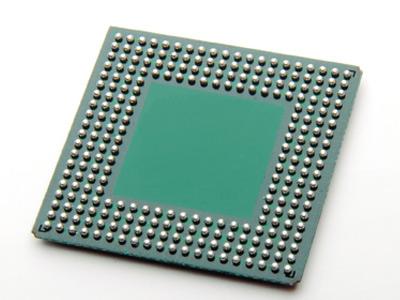
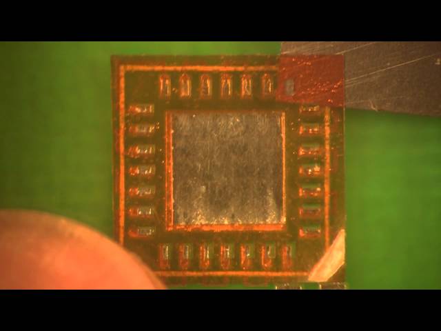
BGA Reballing and Solder Bumping for all types of SMD's Lead, Lead Free and Solder Alloy Conversion. Package types include but are not limited to: PBGA (Plastic Ball Grid Array) TBGA (Tape Ball Grid Array) uBGA (Micro BGA) CCGA (Ceramic Colum
New Equipment | Rework & Repair Equipment
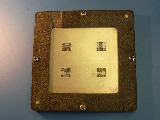
Custom made reballing fixtures designed for your specific component. Allows for high yield reballing of multiple parts at one time. Use for ball attach to BGA components and for solder bumping of LGA's and QFN's. Simply send us the data sheet and
Electronics Forum | Thu Oct 08 14:04:04 EDT 1998 | Kris Ewen
Manish, I've seen similar phenomenon when processing CSPs on our cards. In our case, we were placing the components over the opening to in-pad blind vias. Due to poor drilling and plating processes by our board suppliers, volatiles were outgassing
Electronics Forum | Wed Oct 07 15:25:02 EDT 1998 | Joe P.
Hi Everybody | | Is anyone aware of the possible causes that may lead to voids in the solder bumps after assembly. We assembled some dice on thin substrates and after assembly, void formation in the solder bumps were observed. | We have alread
Used SMT Equipment | Semiconductor & Solar
Bondtester by DAGE, in good condition. DAGE Series 4000 Bondtester product information. The 4000 bondtester is multipurpose, capable of performing all pull and shear applications. The 4000 bondtester can be configured as a simple bond wire pull
Used SMT Equipment | Pick and Place/Feeders
60,000cph with a large component range of 0201 to 30mmx30mm. Flexible, high-speed productivity for medium volume environments. A powerful line booster solution or high-performance small part placer. Dual-beam, dual-drive overhead gantry system
Industry News | 2012-03-08 22:21:34.0
The SMTA is pleased to announce the program for the 2012 International Conference on Soldering and Reliability being held May 15-18 in Toronto, Ontario, Canada. Following on the very successful 2005 and 2006 International Conferences on Lead-free Soldering, and the SMTA International Conference on Soldering and Reliability held in Toronto since 2007, this conference will bring together the community of soldering and reliability experts. The event will be co-located with the SMTA Lead-Free Academy and the SMTA Toronto Expo.
Industry News | 2018-10-18 10:40:04.0
Via Tent-Holes with Solder Mask
Technical Library | 2024-02-02 07:48:31.0
Maximizing Efficiency: The High-Speed SMT Line With Laser Depanelizer In today's rapidly evolving electronics manufacturing landscape, optimizing efficiency, cost-effectiveness, and precision remains paramount. Businesses engaged in producing industrial control boards, computer motherboards, mobile phone motherboards, and mining machine boards face ongoing challenges in streamlining production processes. The integration of expensive equipment strains budgets, making the creation of an efficient, cost-effective high-speed SMT line a daunting task. However, a solution exists that seamlessly combines these elements into a singular, high-performance, and cost-effective SMT line. Let's delve into the specifics. A Comprehensive High-Speed SMT Line Our innovative solution amalgamates two pivotal components: a cutting-edge SMT (Surface Mount Technology) production line and a laser cutting line equipped with a depanelizer. The SMT Production Line The high-speed SMT line comprises several essential components, each fulfilling a unique role in the manufacturing process: 1. PCB Loader: This initial stage involves loading boards onto the production line with utmost care. Our Board Loader prioritizes safety, incorporating various safety light curtains and sensors to promptly halt operations and issue alerts in case of any anomalies. 2. Laser Marking Machine: Every PCB receives a unique two-dimensional code or barcode, facilitating comprehensive traceability. Despite the high-temperature laser process potentially leading to dust accumulation on PCB surfaces, our dedicated PCB Surface Cleaner swiftly addresses this issue. 3. SMT Solder Paste Printer: This stage involves applying solder paste to the boards, a fundamental step in the manufacturing process. 4. SPI (Solder Paste Inspection): Meticulous inspections are conducted at this stage. Boards passing inspection proceed through the NG (No Good) Buffer Conveyor to the module mounters. Conversely, "No Good" results prompt storage of PCBs in the NG Buffer Conveyor, capable of accommodating up to 25 PCBs. Operators can retrieve these NG boards for rework after utilizing our specialized PCB Mis Cleaner to remove solder paste. 5. Module Mounters: These machines excel in attaching small and delicate components, necessitating precision and expertise in the module mounting process. 6. Standard Pick And Place Machines: The selection of these machines is contingent upon your specific BOM (Bill of Materials) list. 7. Pre-Reflow AOI (Automated Optical Inspection): Boards undergo examination for component quality at this stage. Detected issues prompt the Sorting Conveyor to segregate boards for rework. 8. Reflow Oven: Boards undergo reflow soldering, with our Lyra series reflow ovens recommended for their outstanding features, including nitrogen capability, flux recycling, and water cooling function, ensuring impeccable soldering results. 9. Post-Reflow AOI: This stage focuses on examining soldering quality. Detected defects prompt the Sorting Conveyor to segregate boards for further inspection or rework. Any identified defects are efficiently addressed with the BGA rework station, maintaining the highest quality standards. 10. Laser Depanelizer: Boards advance to the laser depanelizer, where precision laser cutting, often employing green light for optimal results, ensures smoke-free, highly accurate separation of boards. 11. PCB Placement Machine: Cut boards are subsequently managed by the PCB Placement Machine, arranging them as required. With this, all high-speed SMT line processes are concluded. Efficiency And Output This production line demonstrates exceptional productivity when manufacturing motherboards with approximately 3000 electronic components, boasting the potential to assemble up to 180 boards within a single hour. Such efficiency not only enhances output but also ensures cost-effectiveness and precision in your manufacturing processes. At I.C.T, we specialize in crafting customized SMT production line solutions tailored to your product and specific requirements. Our equipment complies with European safety standards and holds CE certificates. For inquiries or to explore our exemplary post-sales support, do not hesitate to contact us. The I.C.T team is here to elevate your electronics manufacturing to new heights of efficiency and cost-effectiveness.
Technical Library | 2007-11-29 17:20:31.0
Programs have been developed to predict the expected yield of flip chip assemblies, based on substrate design and the statistics of actual manufactured boards, as well as placement machine accuracy, variations in bump sizes, and possible substrate warpage. These predictions and the trends they reveal can be used to direct changes in design so that defect levels will fall below the acceptable limits. Shapes of joints are calculated analytically, or when this is not possible, numerically by means of a public domain program called Surface Evolver. The method is illustrated with an example involving the substrate for a flip chip BGA.
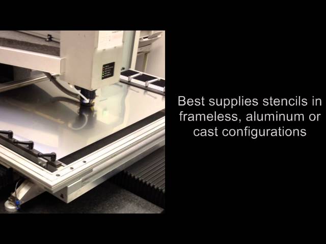
BEST manufactures and designs SMT stencils-both metal and plastic film type. This video demonstrates our metal stencil laser. See more on stencils here: http://www.soldertools.net/categories/Metal-Stencils/
Training Courses | | | PCB Rework and Hand Soldering Courses
The PCB rework and hand soldering courses courses cover techniques of rework and repair of PCBs, BGAs and other electronics assemblies, and teach fundamentals of soldering of electronics assemblies.
Training Courses | | | PCB Rework and Hand Soldering Courses
The PCB rework and hand soldering courses courses cover techniques of rework and repair of PCBs, BGAs and other electronics assemblies, and teach fundamentals of soldering of electronics assemblies.
Events Calendar | Wed Aug 16 00:00:00 EDT 2017 - Sat Aug 19 00:00:00 EDT 2017 | Harbin, China
ICEPT 2017, The 18th International Conference on Electronic Packaging Technology
Career Center | Erode, Tamilnadu India | Engineering
Professional Summary 3+ years of experience in the PCB CAM engineering Exposure to FRONTLINE GENESIS 2000 Having exposure in UCAM Exposure to Create, Array & Panelize it for manufacturability Experienced in Creating impedance cou
Career Center | Fort Worth, Texas USA | Engineering,Maintenance,Production,Quality Control,Research and Development
A mechanically-inclined, results-oriented, lean-driven professional with proven success in implementing programs that result in efficiencies and cost savings. Effectively communicates with diverse audiences, encourages training and employee developme
Processing and Troubleshooting SMT, BGA, CSP and Flip Chip
PCB Libraries, Inc. | https://www.pcblibraries.com/forum/RSS_courtyard-roundoff_topic2380.xml
;Change the values to whatever you want for your personal custom library creation. Courtyard Roundoff : In BGA: The Courtyard Place Round-off... Author: BatiskaffSubject: 2380Posted: 03 Sep 2018 at 2:03amIn BGA
Imagineering, Inc. | https://www.pcbnet.com/blog/hdi-pcb-advantages-and-applications/
. This type of PCB technology allows for improved functionality in smaller consumer products, denser BGA and QFP packages, and lowered heat transfer induced stress


