
Flux application using the DispenseJet® pump is a superior alternative to screen printing and ultrasonic spray. Jet dispensing eliminates the overspray and material waste associated with ultrasonic and spray application methods. Flux application usi
New Equipment | Rework & Repair Services
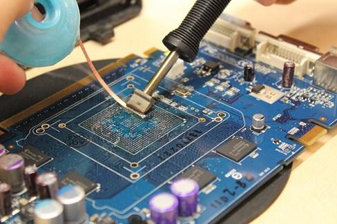
Your BEST Source For High Quality Industry-Leading BGA Repair Service BEST provides industry-leading solutions for Ball Grid Array BGA Repair Services and other grid array device reworks. Our engineers have developed better processes to make our BGA
Electronics Forum | Fri Jun 08 07:52:13 EDT 2007 | zanolli
We are looking at a specialized method of direct soldering ceramic circuit modules (maybe 40mm square) to a mother board with solder joints on only 2 of the 4 sides. These modules would be oriented horizontally, or mezzanine like, to the mother board
Electronics Forum | Wed Feb 07 09:37:48 EST 2007 | billyd
Had the very same thing happen the first time we used the small QFNs. The aperture for the thermal pad in the center needs to be cut in a grid form, either squares (with around a 10 mil spacing between openings) or circles, like a BGA pattern. Too mu
Industry News | 2018-10-18 08:59:34.0
PRINCIPLE OF SURFACE MOUNT PROCESS(SMT PROCESS)
Industry News | 2018-12-08 03:29:29.0
SMT Dictionary – Surface Mount Technology Acronym and Abbreviation
Technical Library | 2009-11-05 11:17:32.0
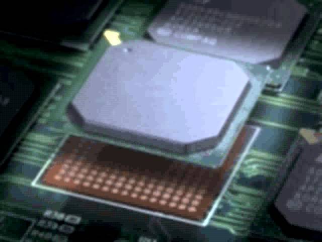
Head-in-pillow (HiP), also known as ball-and-socket, is a solder joint defect where the solder paste deposit wets the pad, but does not fully wet the ball. This results in a solder joint with enough of a connection to have electrical integrity, but lacking sufficient mechanical strength. Due to the lack of solder joint strength, these components may fail with very little mechanical or thermal stress. This potentially costly defect is not usually detected in functional testing, and only shows up as a failure in the field after the assembly has been exposed to some physical or thermal stress.

Flux spray coating on a PCB with uniformal thickness down to 5 microns, with clear edge definition and minimal overspray. Can coat large or shoot dots with the same jet.
This video describes the BEST BGA rework and BGA rework services capabilities. What is described in this movie are the people, processes and tools unique to BEST and how that impacts its customers. The advanced equipment set including multiple refl
Career Center | , Israel | Engineering,Maintenance,Technical Support
I was born on June , 1972 in Khmelnitsky city , Ukraine . I am male. From 1979 to 1987 I was studying at secondary school #7, having finished which I entered the Technical College of Khmelnitsky in specialty Machine Tools with Computer Numeric Contr
Career Center | Rochester, New York USA | Engineering
I have done my undergraduate studies in Mechanical Engineering. I am pursuing my Master's Program in Electronics Packaging. I am currently working as a Research Assistant for RIT-CEMA (Center for Electronics Manufacturing and Assembly). My research
Heller Industries Inc. | https://hellerindustries.com/wp-content/uploads/2018/07/last-will-of-bga-void.pdf
/degradation. Figure 22 (top image) illustrates two BGA corner/outer row solder joints that failed in the typical location at the component/solder joint interface. One of these solder joints (magnified lower image) has a void less than the 25% maximum


