Industry Directory | Consultant / Service Provider / Manufacturer / Research Institute / Laboratory / School
SMT & PCBA Laboratory Services, X-ray inspection, BGA rework, BGA Reballing, Solder Failure Analysis, SMT Assembly Process Validation, SMT Assembly Process Training & Consulting.
Industry Directory | Consultant / Service Provider
Winslow Automation has been advancing lead finish and soldering technology for the military and aeropace, telecommunications, medical, and consumer electronics industry since its inception in 1986.
PROCESS SCIENCES, INC. (PSI) Visit our main Laboratory Services page for more information. Failure Analysis, Material & Process Qualification. We are an analytical services laboratory dedicated to the electronic circuit assembly, printed circu

New Equipment | Education/Training
Our web based seminars represent an efficient way for you and your team to develop practical knowledge, delivering expert advice and guidance to you where, when and how you choose. Simple webinars offer a low cost and time efficient training option.
Electronics Forum | Wed Sep 11 23:20:44 EDT 2002 | scottefiske
Profiles are absolutely the first course of action to validate. A few additional questions would be: * Moisture can cause warping as well, verify the manufacturers recommended handling procedures were followed. * Where is the suspect BGA located
Electronics Forum | Mon Oct 02 20:17:38 EDT 2006 | davef
The different coefficient of expansion of materials used in some BGA can cause warping issues. We've talked about this previously on SMTnet. Search the fine SMTnet Archives. For instance: http://www.smtnet.com/forums/Index.cfm?CFApp=1&Message_ID=2

Used SMT Equipment | X-Ray Inspection
Make: Glenbrook Model: Jewel Box 90T Year: 2016 Type: X-Ray Inspection Details: The Glenbrook JewelBox 90T is a high-resolution, real-time X-ray inspection system designed for precision i

Used SMT Equipment | X-Ray Inspection
• Nordson DAGE VR950 new technology, open, transmissive X-ray tube: -All voltages can reach <0.95 micron feature resolution – The highest voltage is 160KV, target power: 3W -Long service life of filament components -Automatic st
Industry News | 2003-03-20 09:03:05.0
Organizing a Flip Chip and BGA Packaging Technologies Workshop as a part of the SMTA Boston 2003 Conference (June 9-11) at the Bayside Convention Center in Boston, Massachusetts.
Industry News | 2013-07-17 19:05:42.0
IPC — Association Connecting Electronics Industries® will host IPC APEX India™ on 26–29 August 2013 at the NIMHANS Convention Centre in Bangalore, India.
Technical Library | 2008-04-08 17:42:27.0
Concern about the failure of lead-free BGA packages when portable devices such as cell phones are accidentally dropped and a general concern about the resistance of these packages under shock loading has prompted an interest in the impact strength of the soldered BGA connection. This paper reports the results of the measurement of the impact strength of lead-free 0.5±0.01mm diameter BGA spheres on 0.42mm solder mask defined pads on copper/OSP and ENIG substrates using recently developed equipment that can load individual BGA spheres at high strain rates in shear and tension.
Technical Library | 2013-01-03 20:27:54.0
Electronics assemblies with large flip-chip BGA packages can be prone to either pad cratering or brittle intermetallic (IMC) failures under excessive PCB bending. Pad cratering cracks are not detected by electrical testing or non-destructive inspection methods, yet they pose a long term reliability risk since the cracks may propagate under subsequent loads to cause electrical failure. Since the initiation of pad cratering does not result in an instantaneous electrical signature, detecting the onset of this failure has been challenging. An acoustic emission methodology was recently developed by the authors to detect the onset of pad cratering. The instantaneous release of elastic energy associated with the initiation of an internal crack, i.e., Acoustic Emission (AE), can be monitored to accurately determine the onset of both pad cratering and brittle intermetallic (IMC) failures.

Bob Willis "How to Do It" video clip explains how to test BGA or Area Array Packages for solderability. The reason this is difficult to do by other means is the solder terminations would be displaced during solder contact. A simple test like this als

Bob Willis videos show you How to Do It each month. This month we talk about adhesion testing like copper foil, plated copper on PCBs or conformal coating adhesion to board assemblies. Adhesion testing can be used for many different materials and in
Training Courses | | | PCB Assembly Courses
The PCB assembly courses provide knowledge of different processes and equipment used in TH and SMT assembly of printed circuit boards.
Events Calendar | Mon Mar 16 00:00:00 EDT 2020 - Mon Mar 16 00:00:00 EDT 2020 | ,
BGA & Area Array Failures, Causes & Corrective Actions Online Webinar
Events Calendar | Tue Feb 12 00:00:00 EST 2019 - Tue Feb 12 00:00:00 EST 2019 | ,
Webinar: BGA and Area Array Process Defects - Causes & Cures
Career Center | Austin, Texas USA | Production,Quality Control
Join an exciting downstream, solid pre-IPO company in the rolling hills of Austin. Work alongside an elite team of engineers with an excellent track record of success in the telecom industry! Their high-performance networking product technology is g
Career Center | , | Engineering
Job description This position is for a Mechanical Engineer involved in supporting, developing, and improving microelectronics manufacturing processes to optimize Quality, On-Time Delivery, and Cost with an emphasis on Safety. Implementation of Lean M
Career Center | , Minnesota USA | Engineering,Management,Production,Quality Control,Technical Support
Engineer with a diverse background in management, quality, computer and customer service. Experience includes optics, electrical, mechanical, physics, chemistry, process and systems engineering, implementing computers and computer applications for m
Career Center | , Minnesota | Engineering,Management,Production,Quality Control,Technical Support
Engineer with a diverse background in management, quality, computer and customer service. Experience includes optics, electrical, mechanical, physics, chemistry, process and systems engineering, implementing computers and computer applications for m
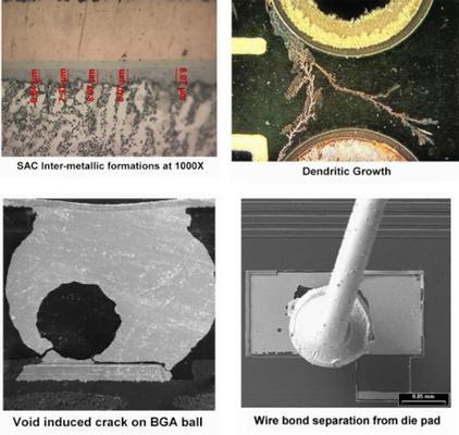
SMTnet Express, October 24, 2019, Subscribers: 32,268, Companies: 10,908, Users: 25,250 Investigation of PCB Failure after SMT Manufacturing Process Credits: ACI Technologies, Inc. An ACI Technologies customer inquired regarding PCB failures
PCB Libraries, Inc. | https://www.pcblibraries.com/Forum/bga-pad-size_topic2607_post10645.html
BGA Pad Size - PCB Libraries Forum Forum Home > PCB Footprint Expert > Questions & Answers New Posts FAQ Search Events Register Login BGA Pad Size
Heller Industries Inc. | https://hellerindustries.com/wp-content/uploads/2018/07/last-will-of-bga-void.pdf
. Statistical T-Test for Solder Joint Voiding Showing Indistinguishable Failure Populations [7] Study #4: S. Sethuraman et al, “The Effect of Process Voiding on BGA Solder Joint Fatigue Life Measured in Accelerated Temperature Cycling” [8


