Supply chain management expert, Zurvahn is an Electronic Manufacturing Service provider for mid- to low-volume products to Original Equipment Manufacturers worldwide.
Industry Directory | Manufacturer
PCBCart, a highly skilled PCB Fab, Parts Sourcing & Assembly services provider for global companies, fabricates 23k+ different PCB designs each year, and are committed on the quality & performance of every circuit board it printed
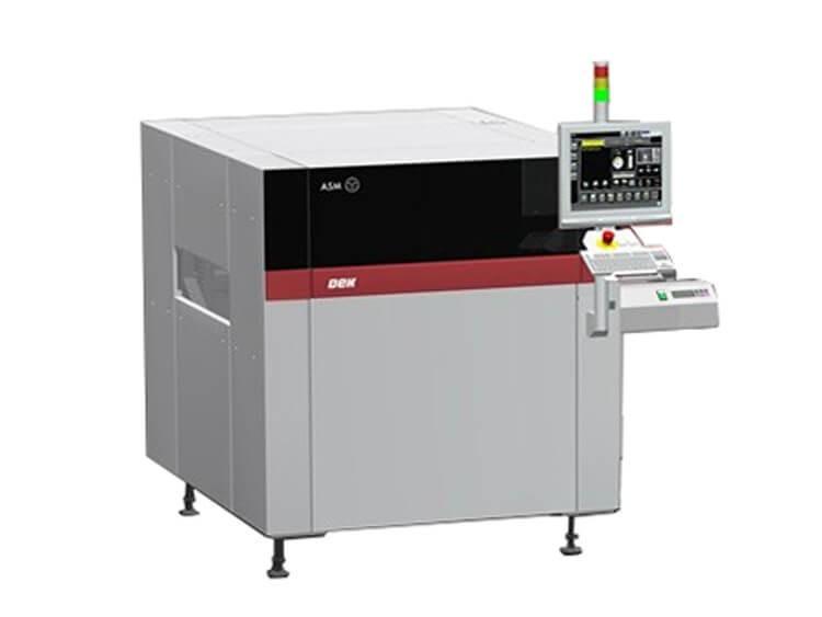
2.0 Cmk @ ± 25 μmProduct description: DEK E Seriels SMT Stencil Printer E by DEK, core cycle time: 8 seconds, Substrate size: 620 mm (X) x 508.5 mm (Y), System alignment capability: > 2.0 Cmk @ ± 25 μm DEK E SMT Stencil Printer DEK E SMT Stenc
New Equipment | Assembly Services
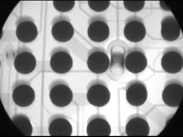
BEST can provide you with analysis services for your BGAs using x-ray equipment. We rework thousands of BGAs and POPs every year, therefore, we have the expertise in BGA X-ray inspection. BEST can be your outsourced BGA x-ray inspection source for o
Electronics Forum | Wed Jan 20 13:07:16 EST 1999 | Robert Noory
I have received prototype PBGA (256 pins) devices from Motorola (actual part number = KXPC850ZT50). These parts seemed very warped on the edges. When I put the part on a plain surface, it rocks quite a bit when I press lightly on a corner. I have
Electronics Forum | Wed Jan 13 19:13:59 EST 1999 | Michael Allen
Just a comment: we've seen PBGAs curl up at the corners, but only on prototype components that came off of a low-volume "prototype" line at our component supplier's lab (non-production overmold material was used). Production parts have not exhibite
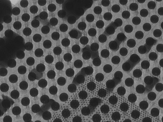
Used SMT Equipment | X-Ray Inspection
we are looking for wth following options: Automatic microfocus X-ray inspection system including: - 160 kV proprietary microfocus X-ray source (open design) with “unlimited” lifetime, including demountable collimator for enhanced image qualit

Used SMT Equipment | Pick and Place/Feeders
PEMTRON SPI TROI-7700HD Technology & Features: Dual Projection Combination of 2D & 3D inspection eliminates common shadow problem with SPI systems. 64 bit Windows 7 Operation System Fast & Stable Operating System for high density PCB.

Parts & Supplies | SPI / Solder Paste Inspection
Quick programming, friendly programming interface Multiple measurement methods True one-button measurement Eight-way motion button, one-click focus Adjustable scanning pitch Solder paste 3D simulation function Powerful SPC function MARK

Parts & Supplies | Repair/Rework
. This machine adopts industrial computer control, full automatic vision alignment system can acquire BGA and the PCB image through the CCD camera and collect them on the image positioning processing system, calculate the offset position and angle th
Technical Library | 2007-11-29 17:20:31.0
Programs have been developed to predict the expected yield of flip chip assemblies, based on substrate design and the statistics of actual manufactured boards, as well as placement machine accuracy, variations in bump sizes, and possible substrate warpage. These predictions and the trends they reveal can be used to direct changes in design so that defect levels will fall below the acceptable limits. Shapes of joints are calculated analytically, or when this is not possible, numerically by means of a public domain program called Surface Evolver. The method is illustrated with an example involving the substrate for a flip chip BGA.
Technical Library | 2017-07-06 15:50:17.0
Head-in-pillow (HiP) is a BGA defect which happens when solder balls and paste can't contact well during reflow soldering. Package warpage was one of the major reasons for HiP formation. In this paper, package warpage was measured and simulated. It was found that the package warpage was sensitive to the thickness of inside chips. A FEM method considering viscoelastic property of mold compound was introduced to simulate package warpage. The CTE mismatch was found contributes to more than 90% of the package warpage value when reflowing at the peak temperature. A method was introduced to measure the warpage threshold, which is the smallest warpage value that may lead to HiP. The results in different atmospheres showed that the warpage threshold was 50μm larger in N2 than that in air, suggesting that under N2 atmosphere the process window for HiP defects was larger than that under air, which agreed with the experiments.
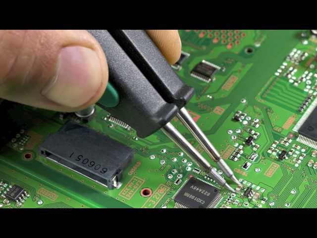
This video presents the capabilities of BEST Inc in terms of its ability to perform high end PCB rework and repair services. BEST Inc., located in Rolling Meadows IL is a company of soldering "geeks". We rework/repair PCBs, train and certify solderin
Events Calendar | Mon Apr 23 00:00:00 EDT 2018 - Thu Apr 26 00:00:00 EDT 2018 | Shanghai, China
SMTA China East Conference 2018
Career Center | Phoenix, Arizona | Engineering,Management,Production,Quality Control,Research and Development,Sales/Marketing,Technical Support
• Highly motivated, solution oriented professional with proven record synergizing scientific, engineering, and business administration backgrounds to drive and sustain customer satisfaction and long term improvements. • Articulate communicator that a
Career Center | Erode, Tamilnadu India | Engineering
Professional Summary 3+ years of experience in the PCB CAM engineering Exposure to FRONTLINE GENESIS 2000 Having exposure in UCAM Exposure to Create, Array & Panelize it for manufacturability Experienced in Creating impedance cou
SMTnet Express, July 6, 2017, Subscribers: 30,558, Companies: 10,626, Users: 23,470 Effects of Package Warpage on Head-in-Pillow Defect Zhenyu Zhao, Chuan Chen, Yuming Wang, Lei Liu, Guisheng Zou, Jian Cai and Qian Wang - Tsinghua University
Heller Industries Inc. | https://hellerindustries.com/wp-content/uploads/2018/07/last-will-of-bga-void.pdf
The Last Will And Testament of the BGA Void THE LAST WILL AND TESTAMENT OF THE BGA VOID David Hillman, Dave Adams, Tim Pearson, Brad Williams, Brittany Petrick, and Ross Wilcoxon Rockwell Collins
Imagineering, Inc. | https://www.pcbnet.com/capabilities/assembly/technology-roadmap/
. Layer Count 50 Max. Working Panel Size 21" x 31" Max. Board Thickness .300" Min. Board Thickness 0.16"(6L) Min. Line/Space • I/L - 2 / 1.5mil (HDI) • O/L - 2 / 1.5 mil (HDI) Warpage .001" / sq. in. BGA Pitch 0.20mm Layer to Layer Registration 3 mil


