
Industry Directory | Training Provider / Manufacturer's Representative / Equipment Dealer / Broker / Auctions / Consultant / Service Provider
Products, services, training & consulting for the assembly, rework & repair of electronic assemblies. BGA process experts. Manufacturers Rep, Distributor & Service Provider for Seamark/Zhuomao and Shuttle Star BGA Rework Stations.
Industry Directory | Manufacturer
We provide cost effective, custom printed circuit boards (PCBs) through an instant online system. We also provide PCB Assemb
New Equipment | Solder Paste Stencils
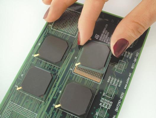
Eliminate hours of solder mask damage repair time for bga sites while improving rework yield. Are you frustrated by the time it takes to repair mask damage underneath the BGA during the rework process? Are you squeezed for space on the PCB in an
New Equipment | Solder Paste Stencils
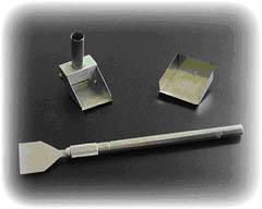
Stentech produces mini stencils; small stencils that are used mainly for BGA re-work. Mini stencils are designed to deposit precise amounts of solder paste for single BGA footprints on loaded PCBs. These precision stencils mimic the footprint and ape
Electronics Forum | Tue Feb 03 14:19:29 EST 2009 | grics
I would agree if you have a board to setup the process. But sometimes this doesn't work... If for some reason if the customers AVL has a Lead Free BGA and I am running Leaded paste (yes this really happens!), you will need to run hotter to get your
Electronics Forum | Thu Oct 11 22:25:50 EDT 2001 | davef
Bruce I�m with yall. Designers and fabricators say �pins�. You say: * BGA pins are 1mm [0.039�] pitch. * BGA pads are 0.4mm [0.0157�] diameter. * BGA pins are 0.6 mm [0.024�] side-to-side. * Board thickness is ~0.4 mm [0.015�] First, as you can
Industry News | 2003-06-25 12:40:26.0
to manufacture and market printed circuit boards utilizing PCB Channel Routing technology from Nortel Networks
Industry News | 2013-01-30 17:54:43.0
Design, assembly, inspection and repair personnel have a new tool to help improve reliability of ball grid arrays (BGAs) and fine-pitch ball grid arrays (FBGAs) in high density applications, thanks to the newly released C revision of IPC-7095, Design and Assembly Process Implementation for BGAs.
Technical Library | 2013-08-01 13:17:44.0
Electronic industry uses a number of metallic materials in various forms. Also new materials and technology are introduced all the time for increased performance. In recent years, corrosion of electronic systems has been a significant issue. Multiplicity of materials used is one reason limiting the corrosion reliability. However, the reduced spacing between components on a printed circuit board (PCB) due to miniaturization of device is another factor that has made easy for interaction of components in corrosive environments. Presently the knowledge on corrosion issues of electronics is very limited. This paper reviews briefly the materials used in electronic systems, factors influencing corrosion, types of corrosion observed in electronics, and testing methods.
Technical Library | 2015-12-23 16:57:27.0
The onset of copper barrel cracks is typically induced by the presence of manufacturing defects. In the absence of discernible manufacturing defects, the causes of copper barrel cracks in printed circuit board (PCB) plated through holes is not well understood. Accordingly, there is a need to determine what affects the onset of barrel cracks and then control those causes to mitigate their initiation.The objective of this research is to conduct a design of experiment (DOE) to determine if there is a relationship between PCB fabrication processes and the prevalence of fine barrel cracks. The test vehicle used will be a 16-layer epoxy-based PCB that has two different sized plated through holes as well as buried vias.
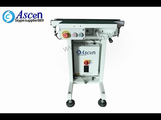
https://www.ascen.ltd/Products/Automatic_SMT_equipment/PCB_conveyor/100.html PCB linking conveyor and PCB belt conveyor mainly used to connect different type PCB board handing equipment effectively for the SMT production line. ASCEN technology is ava
https://www.ascen.ltd/Products/Automatic_SMT_equipment/PCB_conveyor/100.html PCB linking conveyor and PCB belt conveyor mainly used to connect different type PCB board handing equipment effectively for the SMT production line. ASCEN technology is ava
Career Center | Hyderabad, Telangana India | Engineering,Maintenance,Production
Experience in handling Process related issues throughout the Product Manufacturability. Programming and maintenance of SMT Pick and Place Machines of Mirae, Panasonic, NXT and MyData Programming and maintenance of Solder Paste Printer of DEK
Effects of an Appropriate PCB Layout and Soldering Nozzle Design on Quality and Cost Structure in Selective Soldering Processes If you don't see images, please visit online version at: http://www.smtnet.com/express/ Effects
| pcb-services-inc.com&gigaurl=https://precision-pcb-services-inc.com/products/bga-rework-station-wds-750" target="_blank">https://precision-pcb-services-inc.com/products/bga-rework-station-wds-750
WDS-750 SMD & BGA Rework Station – Precision PCB Services, Inc. Search Log in or Create account Cart : 0 Menu Cart 0 Home Catalog Blog About us Log in Create account Search Precision PCB Services, Inc
ASYMTEK Products | Nordson Electronics Solutions | https://www.nordson.com/en/divisions/dage/about/news/live-demonstrations-on-nordson-inspection-systems-at-apex
Live Demonstrations on Nordson Inspection systems at APEX X-Ray Inspection and Test Products Corporate | Global Directory | Languages Division Only All of Nordson Home Products Bondtesting Systems Micro Materials Testing Wafer Inspection and Metrology X-ray Inspection Systems X-ray Counting Systems Applications Battery
Products, services, training & consulting for the assembly, rework & repair of electronic assemblies. BGA process experts. Manufacturers Rep, Distributor & Service Provider for Seamark/Zhuomao and Shuttle Star BGA Rework Stations.
Training Provider / Manufacturer's Representative / Equipment Dealer / Broker / Auctions / Consultant / Service Provider
1750 Mitchell Ave.
Oroville, CA USA
Phone: (888) 406-2830


