New Equipment | Fabrication Services
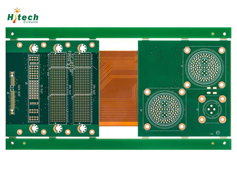
Rigid flex printed circuit boards (PCBs) are manufactured by combining rigid and flexible board technologies. These circuit boards are made up of multiple flexible circuit inner layers. An epoxy pre-preg bonding film is used to attach together these
New Equipment | Assembly Services
PCB Prototype - 2 Layer, Metal Core Board, Hard Gold Plating 30u", With Black Solder Mask - 2 layer, metal core board, hard gold plating 30u", with black solder mask. Advantages: - Metal core board. A PC board to be populated with electronic compo
Industry News | 2003-03-11 08:45:00.0
CAMtastic DXP is the latest version of Altium's complete CAM verification and editing system that bridges the gap between PCB design and manufacturing and facilitates communication between board designers, fabrication engineers, and their clients.
Industry News | 2016-09-14 17:44:33.0
IPC – Association Connecting Electronics Industries® will present “PCB Troubleshooting” on November 2, 2016 in Raleigh, N.C. in conjunction with regional trade show, PCB Carolina.
Technical Library | 2019-09-19 00:28:48.0
The symbiotic relationship between solder masks and selective finishes is not new. The soldermask application is one of the key considerations to ensure a successful application of a selective finish. The selective finish is the final chemical step of the PCB manufacturing process, this is when the panels are at their most valuable and are unfortunately not re-workable. Imperfections are not tolerated, even if they are wholly cosmetic. Quality issues often manifest themselves in the form of a 'ping pong' conversation between the fabricators, the soldermask suppliers and the selective finish suppliers. Without tangible evidence these discussions are difficult to resolve and the selective finish process is usually regarded as responsible. This paper will focus on the chemical characteristics and use them to predict or identify potential issues before they occur rather than specifically name 'critical' soldermasks. It is also the intention of this paper to address the potential of a soldermask to react to common yield hiking practices like UV bumping and oven curing. It is hoped that this awareness will help fabricators to ensure maximum yields by asking the right questions. 'Critical’ soldermasks impact all selective finishes. In this paper, practical experience using immersion tin will be used to highlight the relationship between 'critical' soldermasks and some of the issues seen in the field. The paper will include a novel approach to identify re-deposited volatiles after the reflow.
Technical Library | 2013-12-27 10:39:21.0
The head-in-pillow defect has become a relatively common failure mode in the industry since the implementation of Pb-free technologies, generating much concern. A head-in-pillow defect is the incomplete wetting of the entire solder joint of a Ball-Grid Array (BGA), Chip-Scale Package (CSP), or even a Package-On-Package (PoP) and is characterized as a process anomaly, where the solder paste and BGA ball both reflow but do not coalesce. When looking at a cross-section, it actually looks like a head has pressed into a soft pillow. There are two main sources of head-in-pillow defects: poor wetting and PWB or package warpage. Poor wetting can result from a variety of sources, such as solder ball oxidation, an inappropriate thermal reflow profile or poor fluxing action. This paper addresses the three sources or contributing issues (supply, process & material) of the head-in-pillow defects. It will thoroughly review these three issues and how they relate to result in head-in pillow defects. In addition, a head-in-pillow elimination plan will be presented with real life examples will be to illustrate these head-in-pillow solutions.
Rigid flex printed circuit boards (PCBs) are manufactured by combining rigid and flexible board technologies. These circuit boards are made up of multiple flexible circuit inner layers. An epoxy pre-preg bonding film is used to attach together these

Training Courses | | | PCB Rework and Hand Soldering Courses
The PCB rework and hand soldering courses courses cover techniques of rework and repair of PCBs, BGAs and other electronics assemblies, and teach fundamentals of soldering of electronics assemblies.
Training Courses | | | PCB Rework and Hand Soldering Courses
The PCB rework and hand soldering courses courses cover techniques of rework and repair of PCBs, BGAs and other electronics assemblies, and teach fundamentals of soldering of electronics assemblies.
Events Calendar | Sun Apr 11 18:30:00 UTC 2021 - Sun Apr 11 18:30:00 UTC 2021 | ,
Europe Chapter Webinar: Tombstoning Components during Reflow Soldering - Causes & Cures
Events Calendar | Mon Mar 29 18:30:00 UTC 2021 - Mon Mar 29 18:30:00 UTC 2021 | ,
Juarez Chapter Webinar: DFM, Design For Manufacturing
Career Center | Mesa, Arizona USA | Production
Great opportunity with growing Tempe Company! Temp to hire Class II and III assemblers needed. First shift hours: Monday-Friday 6:45am to 3:15pm (half hour lunch) Second shift hours: Monday-Friday 3:30pm to 12:00am (half hour lunch) Class II s
SMT Express, Volume 5, Issue No. 8 - from SMTnet.com Equipment Impacts of Lead Free Wave Soldering The popular tin (Sn) rich lead free solders are causing severe corrosion to many of the materials used in today�s Wave Solder systems
Imagineering, Inc. | https://www.pcbnet.com/blog/what-is-solder-mask-color-selecting-the-right-option-for-your-product/
PCB Solder Mask Colors: Selecting the Right Option Skip to main content Resources Support Contact Us FAQs Live Chat My Account 847-806-0003 Menu PCB Capabilities Fabrication Technology Roadmap Materials Available HDI
PCB Libraries, Inc. | https://www.pcblibraries.com/forum/txs02612rtwr-footprint-issues_topic2244_post9285.html
) Top Layer Location : [X = 1121.95mm][Y = 648.925 mm]" Unable to apply "solder mask/paste expansion" rules to pads when footprint placed on PCB
.jpg)


