
Industry Directory | Manufacturer
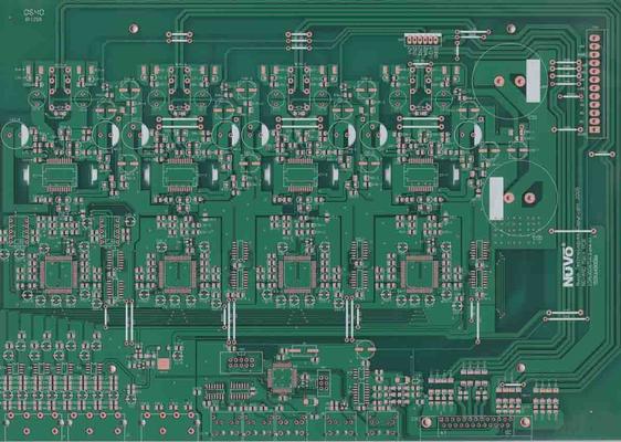
XPCB is a PCB manufacturer with superior expertise in multilayer rigid-flex PCB and flex PCB, supporting special technology including VIPPO, stacked vias, buried vias, blind vias, unsymmetrical structure, and air gap structure.
Industry Directory | Manufacturer
UWELLPCB.com is the PCB supplier. We offer PCB from single side board, double side PCB to 32layer board,including the Rigid PCB, Flex PCB, Rigid-flex PCB,Quick-turn prototype and PCB assembly
New Equipment | Education/Training
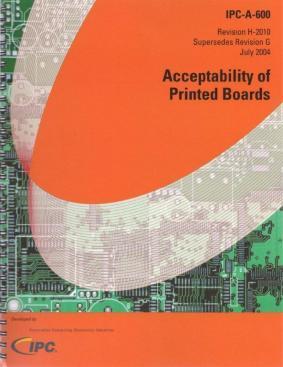
This specification covers qualification and performance of rigid PCBs including with or without plated-through holes, single-sided, double-sided, multilayer with or without blind/buried vias and metal core boards. It addresses final finish and surfac
New Equipment | Education/Training
IPC A-600H Acceptability of Electronic Assemblies. The IPC-A-600, "Acceptability of Printed Boards " is the most widely used published specification on printed wiring boards. This specification has set the standard for rigid printed boards in terms o
Electronics Forum | Mon Feb 19 22:56:20 EST 2007 | davef
Russ We agree with your comments on plugging from one side only. But... We believe that it IS possible to trap process chemicals [technically, not flux] in a blind [or any other] via. This can be done by plating the via closed, rather than pluggi
Electronics Forum | Sat Aug 27 09:47:05 EDT 2005 | davef
From the pic, we see blistering, but none so close to via that we'd attribute the blistering to via, via plugging, or anything of the sort. When we see blisters like this, we think of a surface contaminant being present on the boards at the time of
Industry News | 2003-03-11 08:45:00.0
CAMtastic DXP is the latest version of Altium's complete CAM verification and editing system that bridges the gap between PCB design and manufacturing and facilitates communication between board designers, fabrication engineers, and their clients.
Industry News | 2019-02-19 19:38:20.0
PCB Technology Trends 2018, a new global study published by IPC is now available. The survey-based study shows how printed circuit board (PCB) manufacturers are meeting today’s technology demands and looks at the changes expected by 2023 that will affect the whole industry.
Technical Library | 2013-03-07 18:25:36.0
The market for high-layer-count printed circuit boards (PCB) containing blind and buried vias was once relatively small, and focused on specialized applications in the military and high end computing. The demand for these types of PCBs today is being driven by an increasing number of commercial applications in the telecommunications and semiconductor test market segments. These applications typically require high-aspect-ratio plated-through-holes (PTHs) and blind and buried vias in order to meet the applications interconnect density requirements. Blind and buried vias and high aspect ratio PTHs continue to present manufacturing challenges and frequently are the limiting features to achieving high fabrication yield... First published in the 2012 IPC APEX EXPO technical conference proceedings
Technical Library | 2019-07-17 17:56:34.0
The increased demand for electronic devices in recent years has led to an extensive research in the field to meet the requirements of the industry. Electrolytic copper has been an important technology in the fabrication of PCBs and semiconductors. Aqueous sulfuric acid baths are explored for filling or building up with copper structures like blind micro vias (BMV), trenches, through holes (TH), and pillar bumps. As circuit miniaturization continues, developing a process that simultaneously fills vias and plates TH with various sizes and aspect ratios, while minimizing the surface copper thickness is critical. Filling BMV and plating TH at the same time, presents great difficulties for the PCB manufactures. The conventional copper plating processes that provide good via fill and leveling of the deposit tend to worsen the throwing power (TP) of the electroplating bath. TP is defined as the ratio of the deposit copper thickness in the center of the through hole to its thickness at the surface. In this paper an optimization of recently developed innovative, one step acid copper plating technology for filling vias with a minimal surface thickness and plating through holes is presented.
This video describes the IPC A-600 training and certification program. The IPC A-600 specification is a set of acceptability specifications for printed circuit boards. These standards determine the acceptance and reject criteria for printed wiring bo
SMTnet Express March 7, 2013, Subscribers: 26214, Members: Companies: 13311, Users: 34412 PTH Core-to-Core Interconnect Using Sintered Conductive Pastes The market for high-layer-count printed circuit boards (PCB) containing blind and buried vias
SMTnet Express, July 18, 2019, Subscribers: 32,162, Companies: 10,836, Users: 24,951 Via Fill and Through Hole Plating Process with Enhanced TH Microdistribution Credits: MacDermid Inc. The increased demand for electronic devices in recent years
Imagineering, Inc. | https://www.pcbnet.com/quote/board-quote/?cpn=0
Fabrication Quote – Imagineering Back to Imagineering New Quote login Login Create Account Input your PCB fabrication specifications below and


